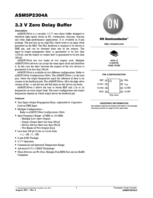
Datasheet4U Logo Datasheet4U.com

ASM5P2304A - 3.3V Zero Delay Buffer

General Description

ASM5P2304A is a versatile, 3.3 V zero delay buffer designed to distribute high speed clocks in PC, workstation, datacom, telecom and other high

performance applications.

pin package.

chip PLL which locks to an input cloc

Key Features

  • Zero Input.
  • Output Propagation Delay, Adjustable by Capacitive Load on FBK Input.
  • Multiple Configurations.
  • Refer to ASM5P2304A Configurations Table.
  • Input Frequency Range: 10 MHz to 133 MHz.
  • Multiple Low.
  • skew Outputs.
  • Output.
  • Output Skew less than 200 pS.
  • Device.
  • Device Skew less than 500 pS.
  • Two Banks of Two Outputs Each.
  • Less than 200 pS Cycle.
  • to.
  • Cycle Jitter (.

📥 Download Datasheet

Datasheet Details

Part number ASM5P2304A
Manufacturer onsemi
File Size 113.93 KB
Description 3.3V Zero Delay Buffer
Datasheet download datasheet ASM5P2304A Datasheet

Full PDF Text Transcription for ASM5P2304A (Reference)

Note: Below is a high-fidelity text extraction (approx. 800 characters) for ASM5P2304A. For precise diagrams, and layout, please refer to the original PDF.

ASM5P2304A 3.3 V Zero Delay Buffer Description ASM5P2304A is a versatile, 3.3 V zero−delay buffer designed to distribute high−speed clocks in PC, workstation, datacom, te...

View more extracted text
signed to distribute high−speed clocks in PC, workstation, datacom, telecom and other high−performance applications. It is available in 8−pin package. The part has an on−chip PLL which locks to an input clock presented on the REF. The PLL feedback is required to be driven to FBK pin, and can be obtained from one of the outputs. The input−to−output propagation delay is guaranteed to be less than ±250 pS, and the output−to−output skew is guaranteed to be less than 200 pS. ASM5P2304A has two banks of two outputs each. Multiple ASM5P2304A devices can accept the same input clock and distribute it. In this case the skew between