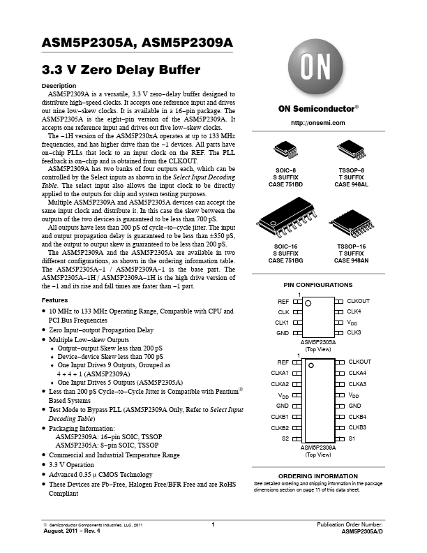
Datasheet4U Logo Datasheet4U.com

ASM5P2309A - 3.3V Zero Delay Buffer

This page provides the datasheet information for the ASM5P2309A, a member of the ASM5P2305A 3.3V Zero Delay Buffer family.

Datasheet Summary

Description

ASM5P2309A is a versatile, 3.3 V zero delay buffer designed to distribute high

speed clocks.

skew clocks.

pin package.

pin version of the ASM5P2309A.

Features

  • 10 MHz to 133 MHz Operating Range, Compatible with CPU and PCI Bus Frequencies.
  • Zero Input.
  • output Propagation Delay.
  • Multiple Low.
  • skew Outputs.
  • Output.
  • output Skew less than 200 pS.
  • Device.
  • device Skew less than 700 pS.
  • One Input Drives 9 Outputs, Grouped as 4 + 4 + 1 (ASM5P2309A).
  • One Input Drives 5 Outputs (ASM5P2305A).
  • Less than 200 pS Cycle.
  • to.
  • Cycle Jitter is Compatible with.

📥 Download Datasheet

Datasheet preview – ASM5P2309A

Datasheet Details

Part number ASM5P2309A
Manufacturer ON Semiconductor
File Size 140.23 KB
Description 3.3V Zero Delay Buffer
Datasheet download datasheet ASM5P2309A Datasheet
Additional preview pages of the ASM5P2309A datasheet.
Other Datasheets by ON Semiconductor

Full PDF Text Transcription

Click to expand full text
ASM5P2305A, ASM5P2309A 3.3 V Zero Delay Buffer Description ASM5P2309A is a versatile, 3.3 V zero−delay buffer designed to distribute high−speed clocks. It accepts one reference input and drives out nine low−skew clocks. It is available in a 16−pin package. The ASM5P2305A is the eight−pin version of the ASM5P2309A. It accepts one reference input and drives out five low−skew clocks. The −1H version of the ASM5P230xA operates at up to 133 MHz frequencies, and has higher drive than the −1 devices. All parts have on−chip PLLs that lock to an input clock on the REF. The PLL feedback is on−chip and is obtained from the CLKOUT. ASM5P2309A has two banks of four outputs each, which can be controlled by the Select inputs as shown in the Select Input Decoding Table.
Published: |