Datasheet4U Logo Datasheet4U.com

NB3N4666C - 3.3 V Quad LVCMOS Differential Line Receiver Translator

Datasheet Summary

Description

The NB3N4666C is a quad

offering data rates up to 400 Mbps (200 MHz) and low power consumption.

safe protection circuit that provides a known output voltage under input open circuit, short an

Features

  • Accepts M.
  • LVDS, LVDS, LVPECL and HCSL Differential Input Signal Levels.
  • Maximum Data Rate of 400 Mbps.
  • Maximum Clock Frequency of 200 MHz.
  • 25 ps Typical Channel.
  • to.
  • Channel Skew.
  • 3.3 ns Maximum Propagation Delay.
  • 3.3 V ±10% Power Supply.
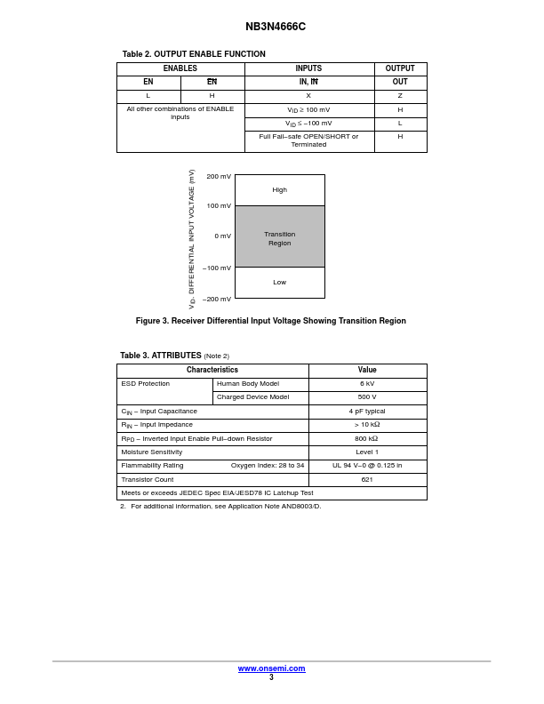
  • High Impedance Outputs When Disabled.
  • Low Quiescent Power < 10 mW Typical.
  • Supports Open, Short, and Terminated Input Fail.
  • safe.
  • 40.

📥 Download Datasheet

Datasheet preview – NB3N4666C

Datasheet Details

Part number NB3N4666C
Manufacturer ON Semiconductor
File Size 117.89 KB
Description 3.3 V Quad LVCMOS Differential Line Receiver Translator
Datasheet download datasheet NB3N4666C Datasheet
Additional preview pages of the NB3N4666C datasheet.
Other Datasheets by ON Semiconductor

Full PDF Text Transcription

Click to expand full text
NB3N4666C 3.3 V Quad LVCMOS Differential Line Receiver Translator Description The NB3N4666C is a quad−channel LVDS line receiver/translator offering data rates up to 400 Mbps (200 MHz) and low power consumption. The NB3N4666C receiver incorporates input fail−safe protection circuit that provides a known output voltage under input open−circuit, short and terminated (100 W) conditions. The four independent inputs accept differential signals such as: M−LVDS, LVDS, LVPECL and HCSL and translates them to a single−ended, 3.3 V LVCMOS. The NB3N4666C also offers active high and active low enable/disable inputs (EN and EN) that allow users to control outputs of all four receivers.
Published: |