Datasheet4U Logo Datasheet4U.com

NB3N502 - 14 MHz to 190 MHz PLL Clock Multiplier

Datasheet Summary

Description

TTL/CMOS level output clock which is a precise multiple of the external input reference clock signal source.

The device is a cost efficient replacement for the crystal oscillators commonly used in electronic systems.

Features

  • Clock Output Frequency up to 190 MHz.
  • Operating Range: VDD = 3 V to 5.5 V.
  • Low Jitter Output of 15 ps One Sigma (rms).
  • Zero ppm Clock Multiplication Error.
  • 45%.
  • 55% Duty Cycle.
  • 25 mA TTL.
  • level Drive Outputs.
  • Crystal Reference Input Range of 5.
  • 27 MHz.
  • Input Clock Frequency Range of 2.
  • 50 MHz.
  • Available in 8.
  • pin SOIC Package or in Die Form.
  • Full Industrial Temperat.

📥 Download Datasheet

Datasheet preview – NB3N502

Datasheet Details

Part number NB3N502
Manufacturer ON Semiconductor
File Size 208.89 KB
Description 14 MHz to 190 MHz PLL Clock Multiplier
Datasheet download datasheet NB3N502 Datasheet
Additional preview pages of the NB3N502 datasheet.
Other Datasheets by ON Semiconductor

Full PDF Text Transcription

Click to expand full text
14 MHz to 190 MHz PLL Clock Multiplier NB3N502 
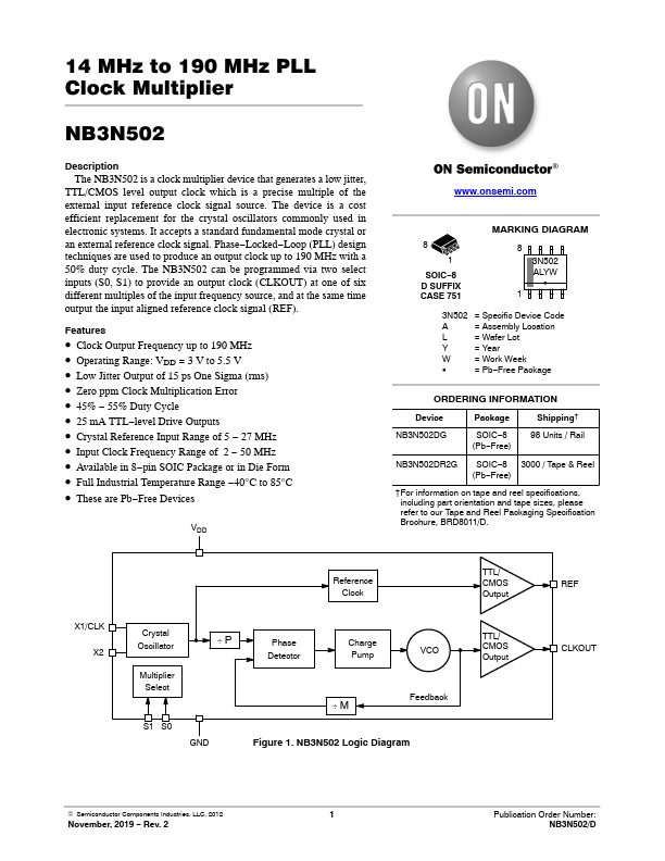
Description The NB3N502 is a clock multiplier device that generates a low jitter, TTL/CMOS level output clock which is a precise multiple of the external input reference clock signal source. The device is a cost efficient replacement for the crystal oscillators commonly used in electronic systems. It accepts a standard fundamental mode crystal or an external reference clock signal. Phase−Locked−Loop (PLL) design techniques are used to produce an output clock up to 190 MHz with a 50% duty cycle. The NB3N502 can be programmed via two select inputs (S0, S1) to provide an output clock (CLKOUT) at one of six different multiples of the input frequency source, and at the same time output the input aligned reference clock signal (REF).
Published: |