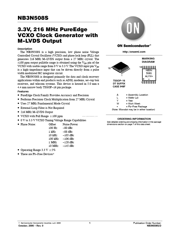
Datasheet4U Logo Datasheet4U.com
onsemi logo

NB3N508S Datasheet

Manufacturer: onsemi
NB3N508S datasheet preview

Datasheet Details

Part number NB3N508S
Datasheet NB3N508S_ONSemiconductor.pdf
File Size 283.80 KB
Manufacturer onsemi
Description PureEdge VCXO Clock Generator
NB3N508S page 2 NB3N508S page 3

NB3N508S Overview

The NB3N508S is a high precision, low phase noise Voltage Controlled Crystal Oscillator (VCXO) and phase lock loop (PLL) that generates 216 MHz M−LVDS output from a 27 MHz crystal. The ±100 ppm output pullable range is obtained using the VIN pin of the VCXO with usable range from 0 V to 3.3 V. The VCXO input pin VIN is a high−impedance input that can be driven directly from a pulse width modulated RC integrator...

NB3N508S Key Features

  • Rev. 0
  • For additional information on our Pb-Free strategy and soldering details, please download the ON Semiconductor Soldering
onsemi logo - Manufacturer

More Datasheets from onsemi

See all onsemi datasheets

Part Number Description
NB3N501 3.3V / 5.0V 13 MHz to 160 MHz PLL Clock Multiplier
NB3N502 14 MHz to 190 MHz PLL Clock Multiplier
NB3N51032 Dual HCSL/LVDS Clock Generator
NB3N51034 Quad HCSL - LVDS Clock Generator
NB3N51044 Quad HCSL / LVDS Clock Generator
NB3N51054 Quad HCSL / LVDS Clock Generator
NB3N511 3.3V / 5.0V 14MHz to 200MHz PLL Clock Multiplier
NB3N551 Ultra-Low Skew 1:4 Clock Fanout Buffer
NB3N5573 Dual HCSL Clock Generator
NB3N106K 3.3V Differential 1:6 Fanout Clock Driver

NB3N508S Distributor

Datasheet4U Logo
Since 2006. D4U Semicon. About Datasheet4U Contact Us Privacy Policy Purchase of parts