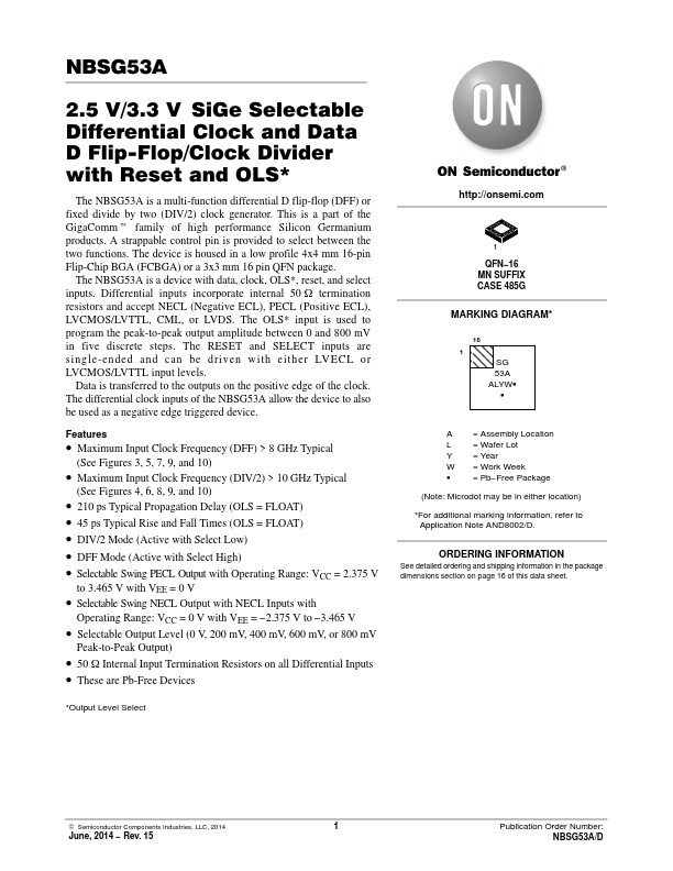
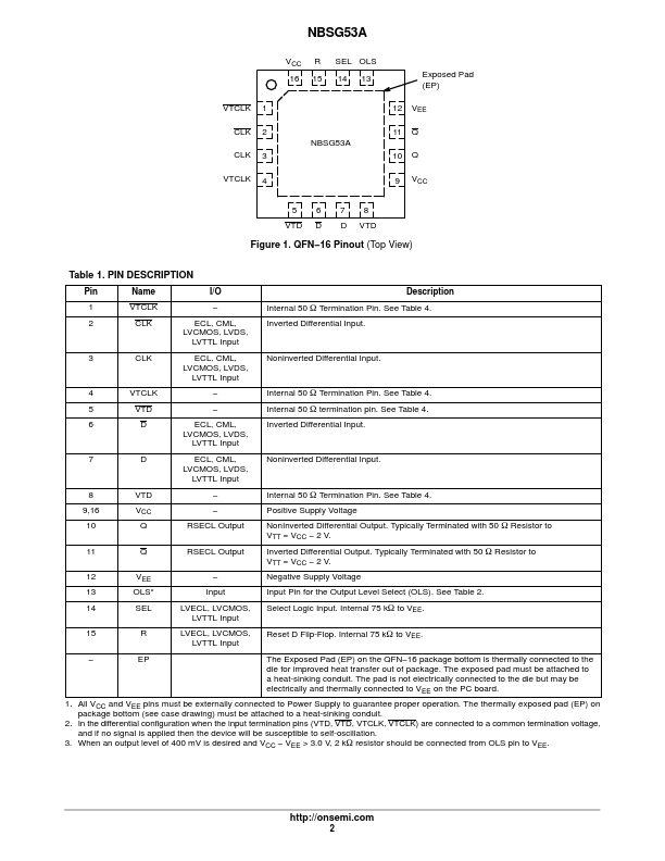
Datasheet4U Logo Datasheet4U.com

NBSG53A - 2.5V/3.3V SiGe Selectable Differential Clock and Data D Flip-Flop/Clock Divider

Description

Pin Name I/O Description 1 VTCLK

Internal 50 W Termination Pin.

See Table 4.

Inverted Differential Input.

Internal 50 W Termination Pin.

Features

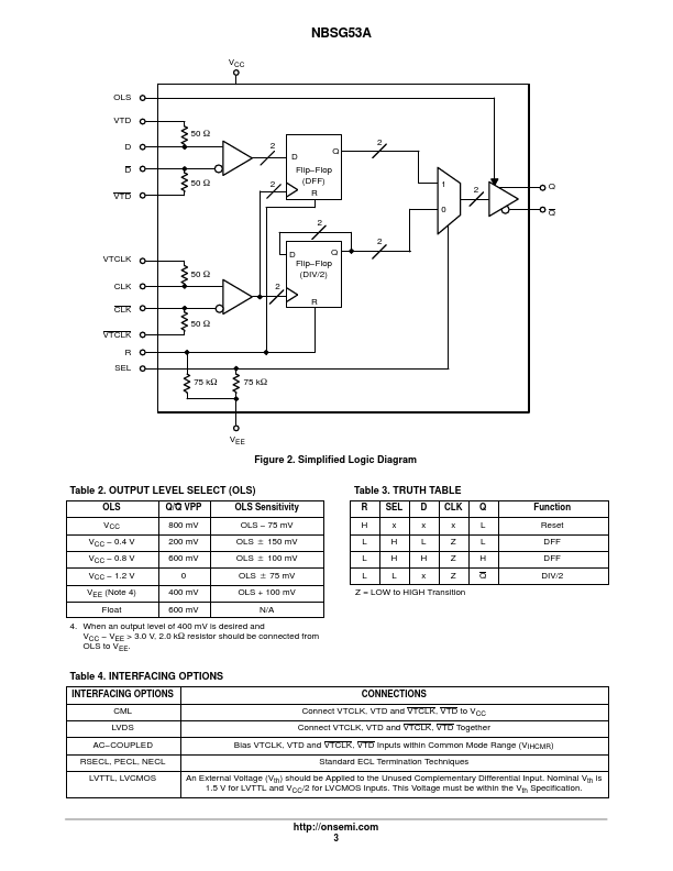
  • Maximum Input Clock Frequency (DFF) > 8 GHz Typical (See Figures 3, 5, 7, 9, and 10).
  • Maximum Input Clock Frequency (DIV/2) > 10 GHz Typical (See Figures 4, 6, 8, 9, and 10).
  • 210 ps Typical Propagation Delay (OLS = FLOAT).
  • 45 ps Typical Rise and Fall Times (OLS = FLOAT).
  • DIV/2 Mode (Active with Select Low).
  • DFF Mode (Active with Select High).
  • Selectable Swing PECL Output with Operating Range: VCC = 2.375 V to 3.465 V with VEE = 0 V.

📥 Download Datasheet

Datasheet preview – NBSG53A

Datasheet Details

Part number NBSG53A
Manufacturer ON Semiconductor
File Size 162.14 KB
Description 2.5V/3.3V SiGe Selectable Differential Clock and Data D Flip-Flop/Clock Divider
Datasheet download datasheet NBSG53A Datasheet
Additional preview pages of the NBSG53A datasheet.
Other Datasheets by ON Semiconductor

Full PDF Text Transcription

Click to expand full text
NBSG53A 2.5 V/3.3 V SiGe Selectable Differential Clock and Data D Flip-Flop/Clock Divider with Reset and OLS* The NBSG53A is a multi-function differential D flip-flop (DFF) or fixed divide by two (DIV/2) clock generator. This is a part of the GigaCommt family of high performance Silicon Germanium products. A strappable control pin is provided to select between the two functions. The device is housed in a low profile 4x4 mm 16-pin Flip-Chip BGA (FCBGA) or a 3x3 mm 16 pin QFN package. The NBSG53A is a device with data, clock, OLS*, reset, and select inputs. Differential inputs incorporate internal 50 W termination resistors and accept NECL (Negative ECL), PECL (Positive ECL), LVCMOS/LVTTL, CML, or LVDS.
Published: |