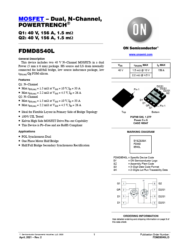
FDMD8540L Description
This device includes two 40 V N−Channel MOSFETs in a dual Power (5 mm x 6 mm) package. HS source and LS drain internally connected for half/full bridge, low source inductance package, low rDS(on)/Qg FOM silicon.
FDMD8540L Key Features
- Max rDS(on) = 1.5 mW at VGS = 10 V, ID = 33 A
- Max rDS(on) = 2.2 mW at VGS = 4.5 V, ID = 26 A
- Max rDS(on) = 1.5 mW at VGS = 10 V, ID = 33 A
- Max rDS(on) = 2.2 mW at VGS = 4.5 V, ID = 26 A
- Ideal for Flexible Layout in Primary Side of Bridge Topology
- 100% UIL Tested
- Kelvin High Side MOSFET Drive Pin-out Capability
- This Device is Pb-Free and are RoHS pliant