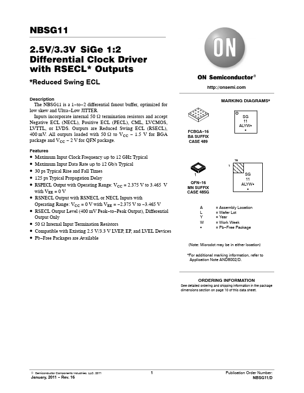
NBSG11 Description
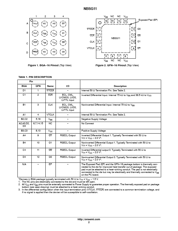
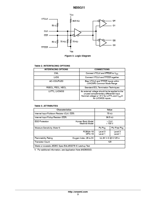
The NBSG11 is a 1−to−2 differential fanout buffer, optimized for low skew and Ultra−Low JITTER. Inputs incorporate internal 50 W termination resistors and accept Negative ECL (NECL), Positive ECL (PECL), CML, LVCMOS, LVTTL, or LVDS. Outputs are Reduced Swing ECL (RSECL), 400 mV.
NBSG11 Key Features
- Maximum Input Clock Frequency up to 12 GHz Typical
- Maximum Input Data Rate up to 12 Gb/s Typical
- 30 ps Typical Rise and Fall Times
- 125 ps Typical Propagation Delay
- RSPECL Output with Operating Range: VCC = 2.375 V to 3.465 V
- RSECL Output Level (400 mV Peak-to-Peak Output), Differential
- 50 W Internal Input Termination Resistors
- patible with Existing 2.5 V/3.3 V LVEP, EP, and LVEL Devices
- Pb-Free Packages are Available
- For additional marking information, refer to Application Note AND8002/D