2SK3547
2SK3547 is Silicon n-channel MOSFET manufactured by Panasonic.
Features
- High-speed switching
- Wide frequency band
- Gate-protection diode built-in
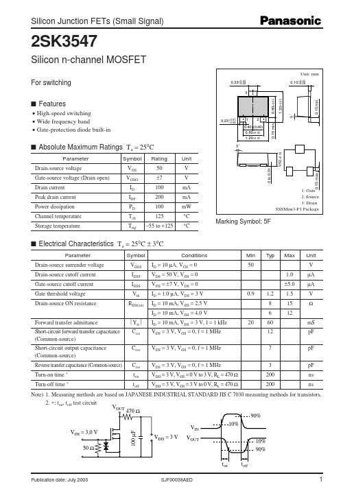
0.33+0.05
- 0.02 3
0.10+0.05
- 0.02
(0.40) (0.40) 0.80±0.05 1.20±0.05 5˚
- Absolute Maximum Ratings Ta = 25°C
Parameter Drain-source voltage Gate-source voltage (Drain open) Drain current Peak drain current Power dissipation Channel temperature Storage temperature Symbol VDS VGSO ID IDP PD Tch Tstg Rating 50 ±7 100 200 100 125
- 55 to +125 Unit V V m A m A m W °C °C
0.15 min.
0.23+0.05
- 0.02
0 to 0.01
0.52±0.03
5˚
1: Gate 2: Source 3: Drain SSSMini3-F1 Package
Marking Symbol: 5F
- Electrical Characteristics Ta = 25°C ± 3°C
Parameter Drain-source surrender voltage Drain-source cutoff current Gate-source cutoff current Gate threshold voltage Drain-source ON resistance Symbol VDSS IDSS IGSS Vth RDS(on) Yfs Ciss Coss Crss ton toff Conditions ID = 10 µA, VGS = 0 VDS = 50 V, VGS = 0 VGS = ±7 V, VDS = 0 ID = 1.0 µA, VDS = 3 V ID = 10 m A, VGS = 2.5 V ID = 10 m A, VGS = 4.0 V Forward transfer admittance Short-circuit forward transfer capacitance (mon-source) Short-circuit output capacitance (mon-source) Reverse transfer capacitance (mon-source) Turn-on time
- Min 50
Typ
Max
Unit V µA µA V Ω
1.0 ±5.0 0.9 1.2 8 6 20 60 12 7 3 200 200 1.5 15 12
ID = 10 m A, VDS = 3 V, f = 1 k Hz VDS = 3 V, VGS = 0, f = 1 MHz VDS = 3 V, VGS = 0, f = 1 MHz VDS = 3 V, VGS = 0, f = 1 MHz VDD = 3 V, VGS = 0 V to 3 V, RL = 470 Ω VDD = 3 V, VGS = 3 V to 0 V, RL = 470 Ω m S p F p F p F ns ns
Turn-off time
- Note) 1. Measuring methods are based on JAPANESE INDUSTRIAL STANDARD JIS C 7030 measuring methods for transistors. 2.
- : ton, toff test circuit VOUT 470 Ω 90% 10% VIN VGS = 3.0 V VDD = 3 V VOUT 10% 50 Ω 90%
100 µF ton
Publication date: July 2003 SJF00038AED toff
0.15 max.
0.15 min.
0.80±0.05
1.20±0.05
PD ...