RJK03C2DPB
Overview
- Pb-free
- Halogen-free * * * *
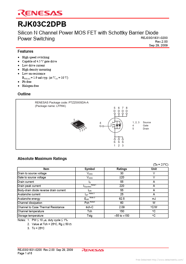
- Outline RENESAS Package code: PTZZ0005DA-A (Package name: LFPAK) 5 6 7 8
- D 5 4 4 G 3 12
| Part Number | Manufacturer | Description |
|---|---|---|
| RJK0329DPB | Renesas | Silicon N Channel Power MOS FET Power Switching |
| RJK0330DPB | Renesas | Silicon N Channel Power MOS FET Power Switching |
| RJK0332DPB | Renesas | Silicon N Channel Power MOS FET Power Switching |
| RJK0351DSP | Renesas | Silicon N Channel Power MOS FET Power Switching |
| RJK0353DPA | Renesas | Silicon N Channel Power MOS FET Power Switching |