Full PDF Text Transcription for RQJ0306FQDQS (Reference)
Note: Below is a high-fidelity text extraction (approx. 800 characters) for
RQJ0306FQDQS. For precise diagrams, and layout, please refer to the original PDF.
RQJ0306FQDQS Silicon P Channel MOS FET Power Switching Features • Low gate drive VDSS : –30 V and 2.5 V gate drive • Low drive current • High speed switching • Small trad...
View more extracted text
5 V gate drive • Low drive current • High speed switching • 
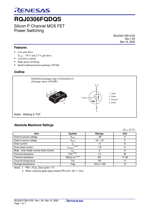
Small traditional power package (UPAK) Outline RENESAS package code: PLZZ0004CA-A (Package name: UPAK R ) 1 2 3 4 1G Notes: Marking is "FQ". Absolute Maximum Ratings Item Symbol Drain to source voltage Gate to source voltage Drain current Drain peak current Body - drain diode reverse drain current Channel dissipation Thermal resistance VDSS VGSS ID ID(pulse) Note1 IDR Pch Note2 Rth(ch-a) Note2 Channel temperature Tch Storage temperature Tstg Notes: 1. PW ≤ 10 µs, Duty cycle ≤ 1% 2. When using the glass epoxy board (FR-4 40 × 40 × 1 mm) REJ03G1780-0100 Rev.1.00 Mar