K4H560838D-TCB3
Features
- Double-data-rate architecture; two data transfers per clock cycle
- Bidirectional data strobe(DQS)
- Four banks operation
- Differential clock inputs(CK and CK)
- DLL aligns DQ and DQS transition with CK transition
- MRS cycle with address key programs -. Read latency 2, 2.5 (clock) .. -. Burst length (2, 4, 8) -. Burst type (sequential & interleave)
- All inputs except data & DM are sampled at the positive going edge of the system clock(CK)
- Data I/O transactions on both edges of data strobe
- Edge aligned data output, center aligned data input
- LDM,UDM/DM for write masking only
- Auto & Self refresh
- 7.8us refresh interval(8K/64ms refresh)
- Maximum burst refresh cycle : 8
- 66pin TSOP II package
DDR SDRAM
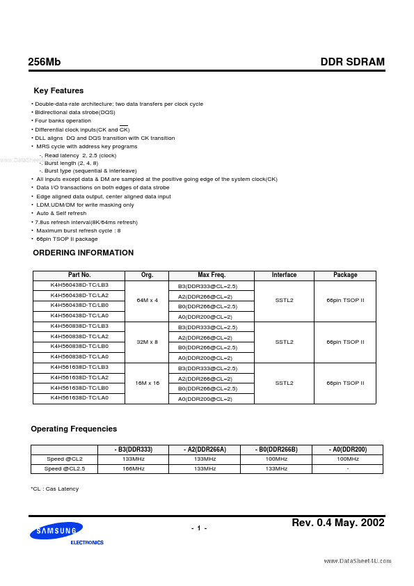
ORDERING INFORMATION
Part No. K4H560438D-TC/LB3 K4H560438D-TC/LA2 K4H560438D-TC/LB0 K4H560438D-TC/LA0 K4H560838D-TC/LB3 K4H560838D-TC/LA2 K4H560838D-TC/LB0 K4H560838D-TC/LA0 K4H561638D-TC/LB3 K4H561638D-TC/LA2 K4H561638D-TC/LB0 K4H561638D-TC/LA0 16M x 16 32M x 8...