Datasheet Details
| Part number | K9F1G08R0A |
|---|---|
| Manufacturer | Samsung Semiconductor |
| File Size | 1.05 MB |
| Description | 128M x 8 Bit / 256M x 8 Bit NAND Flash Memory |
| Datasheet | K9F1G08R0A_Samsungsemiconductor.pdf |
|
|
|
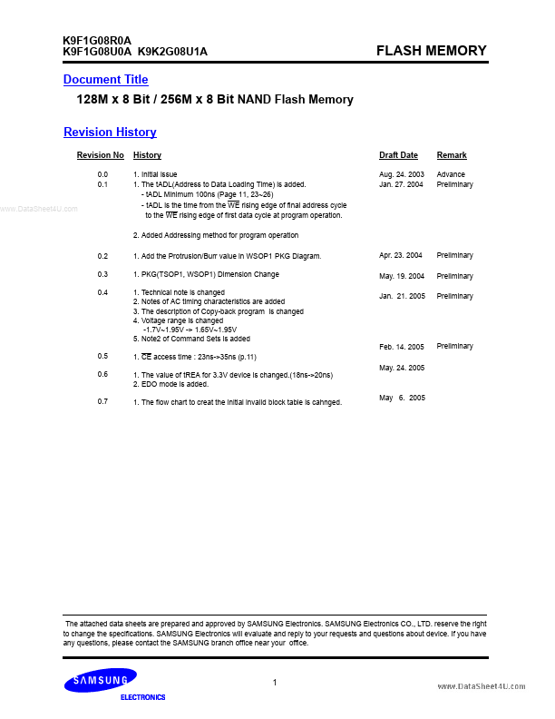
Overview: K9F1G08R0A K9F1G08U0A K9K2G08U1A FLASH MEMORY Document Title 128M x 8 Bit / 256M x 8 Bit NAND Flash Memory Revision History Revision No 0.0 0.1 History 1. Initial issue 1. The tADL(Address to Data Loading Time) is added. - tADL Minimum 100ns (Page 11, 23~26) - tADL is the time from the WE rising edge of final address cycle to the WE rising edge of first data cycle at program operation. 2. Added Addressing method for program operation Draft Date Aug. 24. 2003 Jan. 27. 2004 Remark Advance Preliminary .. 0.2 0.3 0.4 1. Add the Protrusion/Burr value in WSOP1 PKG Diagram. 1. PKG(TSOP1, WSOP1) Dimension Change 1. Technical note is changed 2. Notes of AC timing characteristics are added 3.
| Part number | K9F1G08R0A |
|---|---|
| Manufacturer | Samsung Semiconductor |
| File Size | 1.05 MB |
| Description | 128M x 8 Bit / 256M x 8 Bit NAND Flash Memory |
| Datasheet | K9F1G08R0A_Samsungsemiconductor.pdf |
|
|
|
of Copy-back program is changed 4.
Voltage range is changed -1.7V~1.95V -> 1.65V~1.95V 5.
Note2 of mand Sets is added 1.
| Brand Logo | Part Number | Description | Manufacturer |
|---|---|---|---|
![]() |
K9F1G08R0B | FLASH MEMORY | Samsung Electronics |
| Part Number | Description |
|---|---|
| K9F1G08D0M | 128M x 8 Bit / 64M x 16 Bit NAND Flash Memory |
| K9F1G08Q0A | FLASH MEMORY |
| K9F1G08Q0M | 128M x 8 Bit / 64M x 16 Bit NAND Flash Memory |
| K9F1G08U0A | FLASH MEMORY |
| K9F1G08U0A | 128M x 8 Bit / 256M x 8 Bit NAND Flash Memory |
| K9F1G08U0E | 1Gb E-die NAND Flash |
| K9F1G08U0M | 128M x 8 Bit / 64M x 16 Bit NAND Flash Memory |
| K9F1G16D0M | 128M x 8 Bit / 64M x 16 Bit NAND Flash Memory |
| K9F1G16Q0M | 128M x 8 Bit / 64M x 16 Bit NAND Flash Memory |
| K9F1G16U0M | 128M x 8 Bit / 64M x 16 Bit NAND Flash Memory |