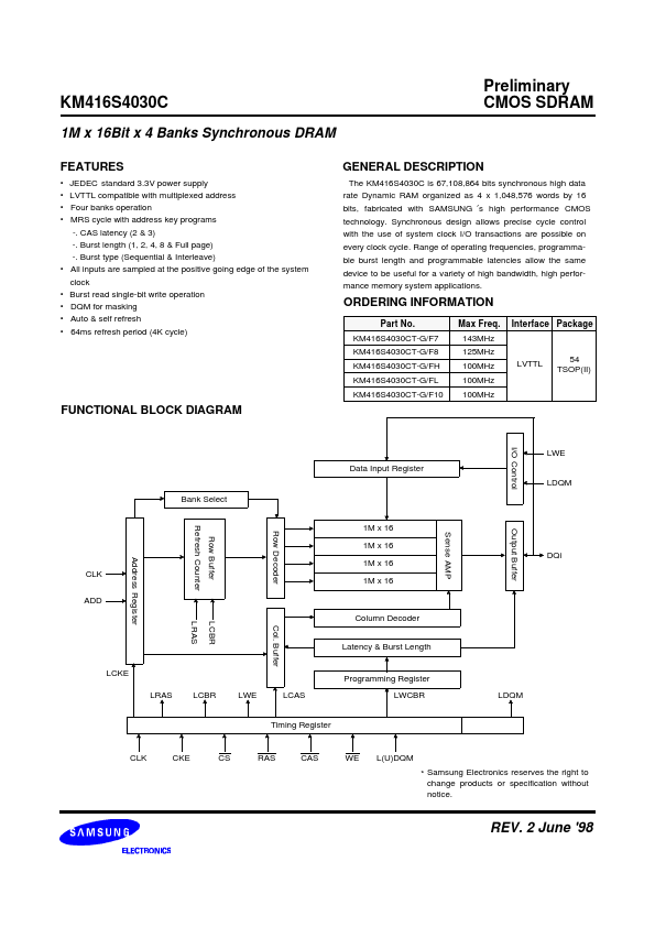
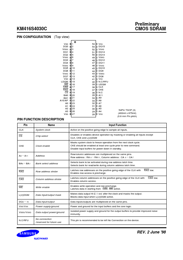
- Part: KM416S4030C
- Description: 1M x 16Bit x 4 Banks Synchronous DRAM
- Manufacturer: Samsung Semiconductor
- Size: 124.27 KB
Related Samsung Semiconductor Datasheets
| Part Number | Description |
|---|---|
| KM416S1020C | 1M x 16 SDRAM |
| KM416S1021C | 512K x 16-Bit x 2-Bank SDRAM |
| KM416S8030 | 2M x 16Bit x 4 Banks Synchronous DRAM |
| KM416S8030B | 128Mbit SDRAM 2M x 16Bit x 4 Banks Synchronous DRAM LVTTL |
| KM416S8030BN | 128Mb SDRAM Shrink TSOP 2M x 16Bit x 4 Banks Synchronous DRAM LVTTL |


