STN6562
STN6562 is 4A Dual N-Channel Enhancement Mode MOSFET manufactured by Stanson Technology.
Dual N Channel Enhancement Mode MOSFET
4.0A
DESCRIPTION
The STN6562 is the dual N-Channel enhancement mode power field effect transistor which is produced using high cell density, DMOS trench technology. This high density process is especially tailored to minimize on-state resistance. These devices are particularly suited for low voltage application, such as cellular phone and notebook puter power management and other battery powered circuits, and low in-line power loss are needed in a very small outline surface mount package.
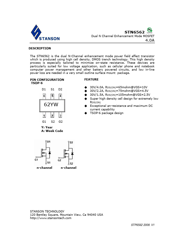
PIN CONFIGURATION TSOP-6
D1 S1 D2
62YW
FEATURE
- 30V/4.0A, RDS(ON)=65mohm@VGS=10V
- 30V/2.2A, RDS(ON)=75mohm@VGS=4.5V
- 30V/1.5A, RDS(ON)=105mohm@VGS=2.5V
- Super high density cell design for extremely low
RDS(ON)
- Exceptional an-resistance and maximum DC current capability
- TSOP-6 package design
G1 S2 G2
Y: Year A: Week Code n-channel n-channel
STANSON TECHNOLOGY 120 Bentley Square, Mountain View, Ca 94040 USA http://.stansontech.
STP6562 2008. V1
Dual N Channel Enhancement Mode MOSFET
4.0A
ABSOULTE MAXIMUM RATINGS (Ta = 25℃ unless otherwise noted )
Parameter
Symbol
Drain-Source Voltage
VDSS
Gate-Source Voltage
VGSS
Continuous Drain Current (TJ=150℃) Pulsed Drain Current
TA=25℃...