TSM7104D
TSM7104D is 20V Dual P-Channel Enhancement Mode MOSFET manufactured by Taiwan Semiconductor.
Features
.. Advanced trench process technology High density cell design for ultra low on-resistance Excellent thermal and electrical capabilities Surface mount Fast switching
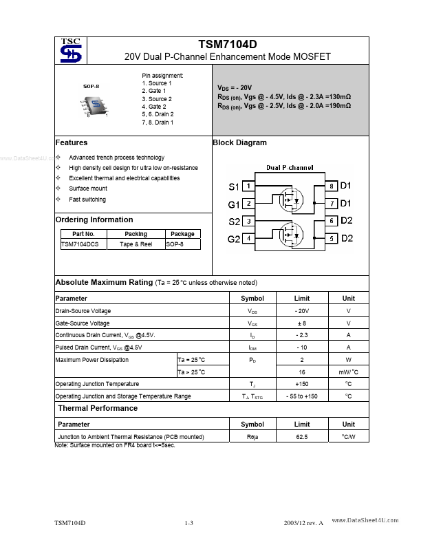
Block Diagram
Ordering Information
Part No. TSM7104DCS Packing Tape & Reel Package SOP-8
Absolute Maximum Rating (Ta = 25 o C unless otherwise noted)
Parameter
Drain-Source Voltage Gate-Source Voltage Continuous Drain Current, VGS @4.5V. Pulsed Drain Current, VGS @4.5V Maximum Power Dissipation Ta = 25 C Ta > 25 C Operating Junction Temperature Operating Junction and Storage Temperature Range TJ TJ, TSTG o o
Symbol
VDS VGS ID IDM PD
Limit
- 20V ±8
- 2.3
- 10 2 16 +150
- 55 to +150
Unit
V V A A W m W/ C o o o
Thermal Performance
Parameter
Junction to Ambient Thermal Resistance (PCB mounted) Note: Surface mounted on FR4 board t<=5sec.
Symbol
Rθja
Limit
Unit o
C/W
1-3
2003/12 rev. A
Electrical Characteristics
Rate ID =
- 2.3A, (Ta = 25 C unless otherwise noted) o
Parameter Static
Drain-Source Breakdown Voltage Drain-Source On-State Resistance Drain-Source On-State
..
Conditions
Symbol
Min
Typ
Max...