SSM3J115TU
SSM3J115TU is Field-Effect Transistor Silicon P-Channel MOS Type manufactured by Toshiba.
..
TOSHIBA Field-Effect Transistor
Silicon P-Channel MOS Type
High-Speed Switching Applications Power Management Switch Applications
- - 1.5 V drive Low ON-resistance: Ron = 353 mΩ (max) (@VGS =
- 1.5 V) Ron = 193 mΩ (max) (@VGS =
- 1.8 V) Ron = 125 mΩ (max) (@VGS =
- 2.5 V) Ron = 98 mΩ (max) (@VGS =
- 4.0 V)
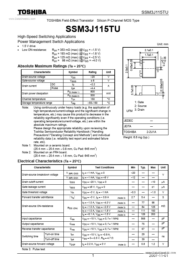
2.0±0.1 2.1±0.1 1.7±0.1 0.65±0.05 +0.1 0.3 -0.05 3 0.166±0.05
Unit:...