Field-Effect Transistor Silicon P-Channel MOS Type
Full PDF Text Transcription (Reference)
The following content is an automatically extracted verbatim text
from the original manufacturer datasheet and is provided for reference purposes only.
View original datasheet text
SSM3J35FS
TOSHIBA Field-Effect Transistor Silicon P-Channel MOS Type
SSM3J35FS
○ High-Speed Switching Applications ○ Analog Switch Applications
• 1.2 V drive • 
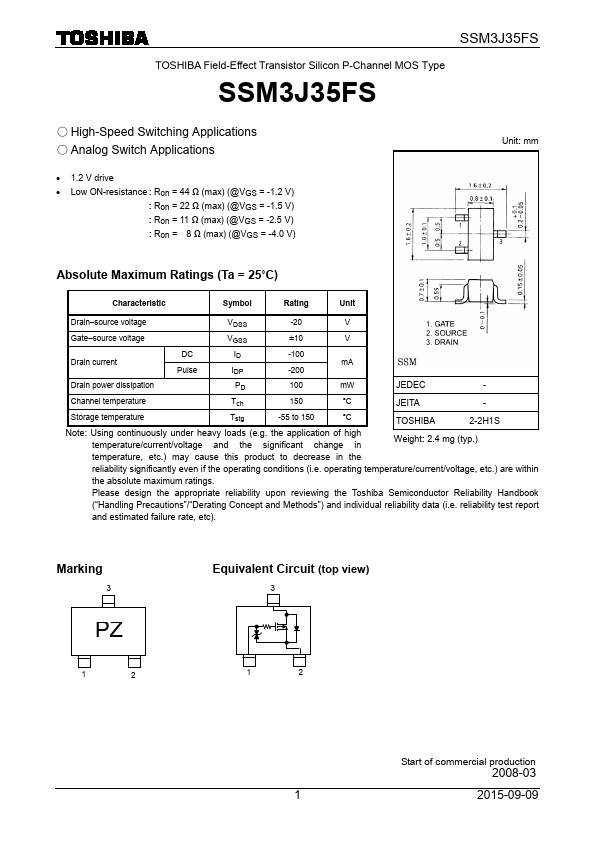
Low ON-resistance : Ron = 44 Ω (max) (@VGS = -1.2 V)
: Ron = 22 Ω (max) (@VGS = -1.5 V) : Ron = 11 Ω (max) (@VGS = -2.5 V) : Ron = 8 Ω (max) (@VGS = -4.0 V)
Unit: mm
Absolute Maximum Ratings (Ta = 25˚C)
Characteristic
Symbol
Rating
Unit
Drain–source voltage
VDSS
-20
V
Gate–source voltage
VGSS
±10
V
Drain current
DC
ID
Pulse
IDP
-100 mA
-200
Drain power dissipation
PD
100
mW
JEDEC
-
Channel temperature
Tch
150
°C
JEITA
-
Storage temperature
Tstg
-55 to 150
°C
TOSHIBA
2-2H1S
Note: Using continuously under heavy loads (e.g.