SSM3K15FS Overview
Key Specifications
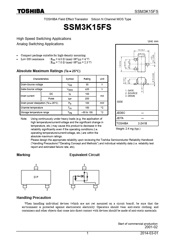
Mount Type: Surface Mount
Pins: 3
Max Operating Temp: 150 °C
Min Operating Temp: -55 °C
Key Features
- Compact package suitable for high-density mounting
- Low ON-resistance
Mount Type: Surface Mount
Pins: 3
Max Operating Temp: 150 °C
Min Operating Temp: -55 °C
| Seller | Inventory | Price Breaks | Buy |
|---|---|---|---|
| Win Source | 82000 | 1565+ : 0.037 USD 3850+ : 0.03 USD 6000+ : 0.0289 USD 8000+ : 0.0289 USD |
View Offer |
| Worldway Electronics | 28412 | 7+ : 0.1488 USD 10+ : 0.1458 USD 100+ : 0.1414 USD 500+ : 0.1369 USD |
View Offer |
| Part Number | Manufacturer | Description |
|---|---|---|
| SSM3K15ACTC | Toshiba | Silicon N-Channel MOSFET |
| SSM3K16CTC | Toshiba | Silicon N-Channel MOSFET |