• Part: SSM3K16TE
  • Description: High Speed Switching Applications Analog Switch Applications
  • Manufacturer: Toshiba
  • Size: 136.57 KB
Download SSM3K16TE Datasheet PDF
Toshiba
SSM3K16TE
SSM3K16TE is High Speed Switching Applications Analog Switch Applications manufactured by Toshiba.
TOSHIBA Field Effect Transistor Silicon N Channel MOS Type High Speed Switching Applications Analog Switch Applications - - 
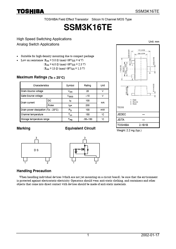
Suitable for high-density mounting due to pact package Low on resistance: Ron = 3.0 Ω (max) (@VGS = 4 V) : Ron = 4.0 Ω (max) (@VGS = 2.5 V) : Ron = 15 Ω (max) (@VGS = 1.5 V) Unit: mm Maximum Ratings (Ta = 25°C) Characteristics Drain-Source voltage Gate-Source voltage Drain current DC Pulse Symbol VDS VGSS ID IDP PD Tch Tstg Rating 20 ±10 100 200 100 150 -55~150 Unit V V m A m W °C °C Drain power dissipation (Ta = 25°C) Channel temperature Storage temperature range JEDEC JEITA TOSHIBA ― ― 2-1B1B Marking Equivalent Circuit Weight: 2.2 mg (typ.) Handling Precaution When handling individual devices (which are not yet mounting on a circuit board), be sure that the environment is protected against electrostatic electricity. Operators should wear anti-static clothing, and containers and other objects that e into direct contact with devices should be made of anti-static materials. 2002-01-17 Electrical Characteristics (Ta = 25°C) Characteristics Gate leakage current Drain-Source breakdown voltage Drain cut-off current Gate threshold voltage Forward transfer admittance Symbol IGSS V (BR) DSS IDSS Vth ½Yfs½ Test Condition VGS = ±10 V, VDS = 0 ID = 0.1 m A, VGS = 0 VDS = 20 V, VGS = 0 VDS = 3 V, ID = 0.1 m A VDS = 3 V, ID = 10 m A ID = 10 m A, VGS = 4 V Drain-Source ON resistance RDS (ON) ID = 10 m A, VGS = 2.5 V ID = 1 m A, VGS = 1.5 V Input capacitance Reverse transfer capacitance Output capacitance Switching time Turn-on time Turn-off time Ciss Crss Coss ton toff VDS = 3 V, VGS = 0, f = 1 MHz VDS = 3 V, VGS = 0, f = 1 MHz VDS = 3 V, VGS = 0, f = 1 MHz VDD = 3 V, ID = 10 m A, VGS = 0~2.5 V Min ¾ 20 ¾ 0.6 40 ¾ ¾ ¾ ¾ ¾ ¾ ¾ ¾ Typ. ¾ ¾ ¾ ¾ ¾ 1.5 2.2 5.2 9.3 4.5 9.8 70 125 Max ±1 ¾ 1 1.1 ¾ 3.0 4.0 15 ¾ ¾ ¾ ¾ ¾ p F p F p F ns W Unit m A V m A V m S Switching Time Test Circuit (a) Test circuit 2.5 V 0 10 ms...