SSM6J26FE
SSM6J26FE is Silicon P-Channel MOSFET manufactured by Toshiba.
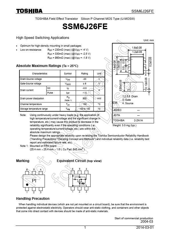
TOSHIBA Field Effect Transistor Silicon P Channel MOS Type (U-MOSIII)
High Speed Switching Applications
Unit: mm
0.2±0.05
- Optimum for high-density mounting in small packages
- Low on-resistance: Ron = 230mΩ (max) (@VGS = -4 V)
Ron = 330mΩ (max) (@VGS = -2.5 V) Ron = 980mΩ (max) (@VGS = -1.8 V)
Absolute Maximum Ratings (Ta = 25°C)
1.6±0.05 1.2±0.05
1.6±0.05 1.0±0.05 0.5 0.5
0.12±0.05
Characteristics
Drain-Source voltage Gate-Source voltage
Drain current
DC Pulse
Drain power dissipation
Channel temperature Storage temperature range
Symbol
Rating
Unit
-20
VGSS
±8
-0.5
-1.5
500 m W
(Note...