products in this document in compliance with all applicable laws and regulations that regulate the inclusion or use of controlled substances. Toshiba assumes no liability for damage or losses occurring as a result of.
The following content is an automatically extracted verbatim text
from the original manufacturer datasheet and is provided for reference purposes only.
View original datasheet text
SSM6J53FE
TOSHIBA Field Effect Transistor Silicon P Channel MOS Type
SSM6J53FE
○ High-Speed Switching Applications ○ Power Management Switch Applications
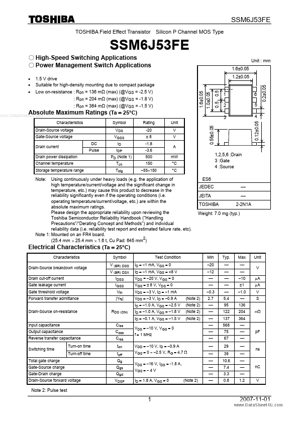
• • • 1.5 V drive Suitable for high-density mounting due to compact package Unit : mm
1.6±0.05 1.2±0.05 0.2±0.05 0.5
1.6±0.05
1.0±0.05
Low on-resistance : Ron = 136 mΩ (max) (@VGS = -2.5 V) : Ron = 204 mΩ (max) (@VGS = -1.8 V) : Ron = 364 mΩ (max) (@VGS = -1.5 V)
Symbol VDS VGSS DC Pulse ID IDP PD (Note 1) Tch Tstg Rating -20 ±8 -1.8 -3.6 500 150 −55~150 Unit V V A mW °C °C
1 2 3
6 5 4 0.12±0.05
www.DataSheet4U.com
Absolute Maximum Ratings (Ta = 25°C)
Characteristics Drain-Source voltage Gate-Source voltage Drain current Drain power dissipation Channel temperature Storage temperature range
0.55±0.