SSM6J771G
SSM6J771G is Silicon P-Channel MOSFET manufactured by Toshiba.
Features
(1) High VGSS voltage : ±12V (2) High VDSS voltage : -20V (3) Low drain-source on-resistance
: RDS(ON) = 26 mΩ (typ.) (@VGS = -4.5 V,ID = -3.0A) RDS(ON) = 24 mΩ (typ.) (@VGS = -8.0 V,ID = -3.0A) RDS(ON) = 23 mΩ (typ.) (@VGS = -8.5 V,ID = -3.0A)
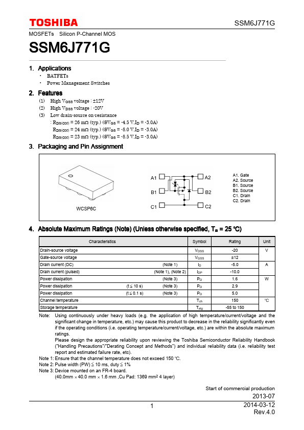
3. Packaging and Pin Assignment
WCSP6C
A1. Gate A2. Source B1. Source B2. Source C1. Drain C2. Drain
4. Absolute Maximum Ratings (Note) (Unless otherwise specified, Ta = 25 )
Characteristics
Symbol
Rating
Unit
Drain-source voltage
VDSS
-20
Gate-source voltage
VGSS
±12
Drain current (DC)
(Note 1)
-5.0
Drain current (pulsed)
(Note 1), (Note 2)
-10.0
Power dissipation
(Note 3)
Power dissipation
(t ≤ 10 s)
(Note 3)
Power dissipation
(t ≤ 0.1 s)
(Note 3)
Channel temperature
Tch...