Datasheet4U Logo Datasheet4U.com

CHA2069-99F - 18-31GHz Low Noise Amplifier

General Description

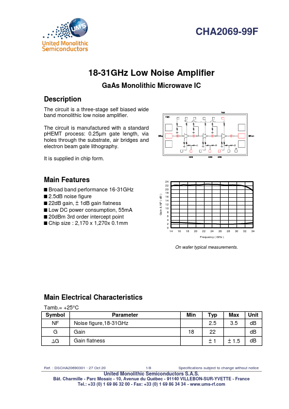
The circuit is a three-stage self biased wide band monolithic low noise amplifier.

The circuit is manufactured with a standard pHEMT process: 0.25µm gate length, via holes through the substrate, air bridges and electron beam gate lithography.

It is supplied in chip form.

Key Features

  • Broad band performance 16-31GHz.
  • 2.5dB noise figure.
  • 22dB gain,  1dB gain flatness.
  • Low DC power consumption, 55mA.
  • 20dBm 3rd order intercept point.
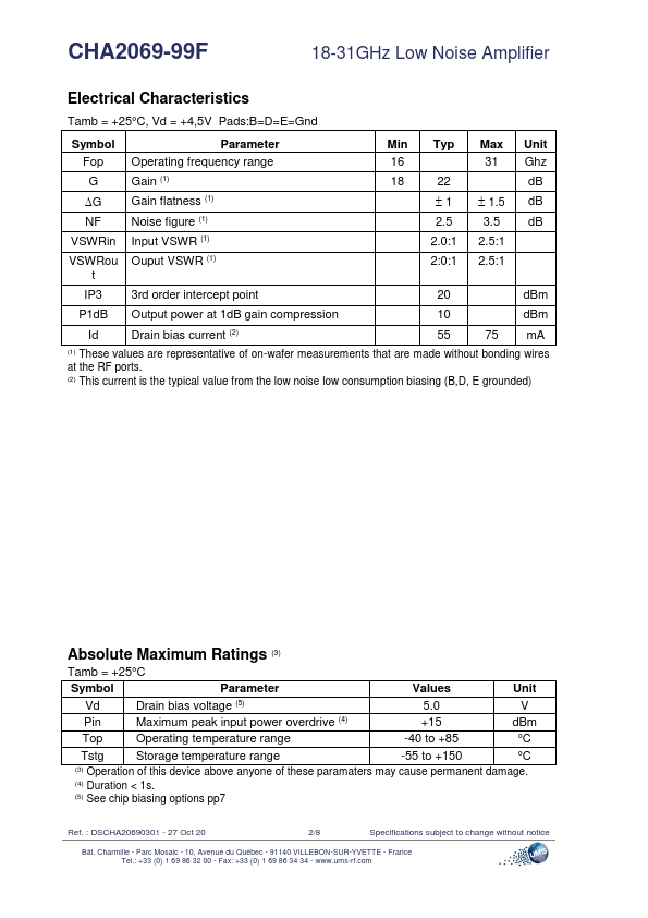
  • Chip size : 2,170 x 1,270x 0.1mm Gain & NF ( dB ) 24 22 20 18 16 14 12 10 8 6 4 2 0 14 16 18 20 22 24 26 28 30 32 34 Frequency ( GHz ) On wafer typical measurements. Main Electrical Characteristics Tamb. = +25°C Symbol Parameter NF Noise figure,18-31GHz G Gain G Gain flatness Min Typ Max Unit 2.5 3.5 dB.

📥 Download Datasheet

Datasheet Details

Part number CHA2069-99F
Manufacturer United Monolithic Semiconductors
File Size 280.84 KB
Description 18-31GHz Low Noise Amplifier
Datasheet download datasheet CHA2069-99F Datasheet

Full PDF Text Transcription (Reference)

The following content is an automatically extracted verbatim text from the original manufacturer datasheet and is provided for reference purposes only.

View original datasheet text
CHA2069-99F 18-31GHz Low Noise Amplifier GaAs Monolithic Microwave IC Description The circuit is a three-stage self biased wide band monolithic low noise amplifier. The circuit is manufactured with a standard pHEMT process: 0.25µm gate length, via holes through the substrate, air bridges and electron beam gate lithography. It is supplied in chip form. Main Features ■ Broad band performance 16-31GHz ■ 2.5dB noise figure ■ 22dB gain,  1dB gain flatness ■ Low DC power consumption, 55mA ■ 20dBm 3rd order intercept point ■ Chip size : 2,170 x 1,270x 0.1mm Gain & NF ( dB ) 24 22 20 18 16 14 12 10 8 6 4 2 0 14 16 18 20 22 24 26 28 30 32 34 Frequency ( GHz ) On wafer typical measurements. Main Electrical Characteristics Tamb.