Datasheet Summary
RoHS PLIANT
18-31GHz Low Noise Amplifier
GaAs Monolithic Microwave IC
Description
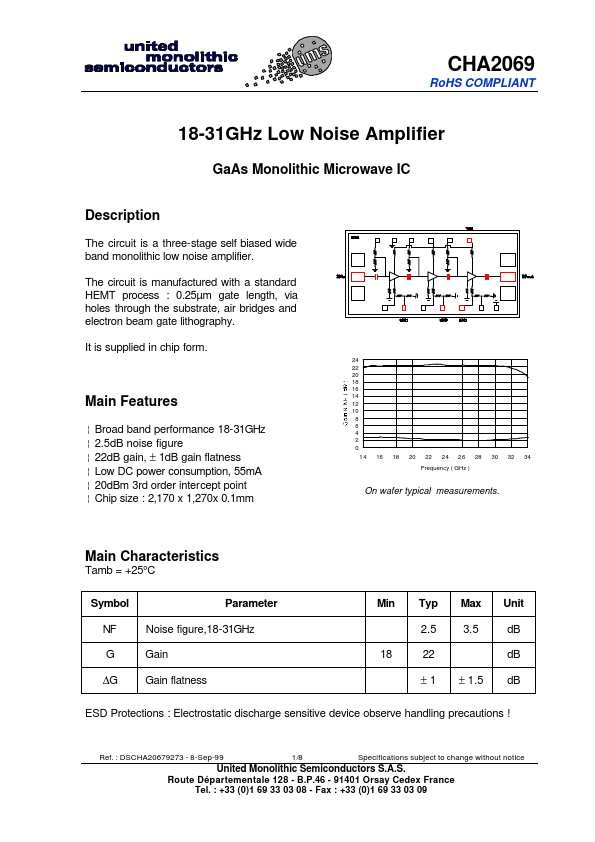
The circuit is a three-stage self biased wide band monolithic low noise amplifier.
The circuit is manufactured with a standard HEMT process : 0.25µm gate length, via holes through the substrate, air bridges and electron beam gate lithography.
It is supplied in chip form.
Main Features
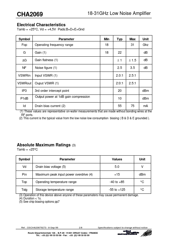
¦ Broad band performance 18-31GHz ¦ 2.5dB noise figure ¦ 22dB gain, ± 1dB gain flatness ¦ Low DC power consumption, 55mA ¦ 20dBm 3rd order intercept point ¦ Chip size : 2,170 x 1,270x 0.1mm
24 22 20 18 16 14 12 10
8 6 4 2 0
14 16 18 20 22 24 26 28 30 32 34
Frequency ( GHz )
On wafer typical measurements.
Main...