Datasheet4U Logo Datasheet4U.com

CHA7114 - X Band High Power Amplifier

Datasheet Summary

Description

CHA7114 is a monolithic two-stage GaAs high power amplifier designed for X band applications.

This device is manufactured using a UMS 0.25 µm power pHEMT process, including, via holes through the substrate and air bridges.

Features

  • 0.25µm Power pHEMT Technology 8.5.
  • 11.5GHz Frequency Range 8W Output Power @ 4dBc High PAE: > 40% @ 4dBc 20dB nominal Gain Quiescent Bias point: Vd = 8V, Id = 2A Chip size: 4.41mm x 3.31mm x 0.07mm Main Characteristics Tamb = +25° C (Tamb is the back-side of the chip) Vd = 8V, Id (Quiescent) = 2A, Pulse width = 25µs, Duty cycle = 10% Symbol Top Fop P_4dBc G Parameter Operating temperature range Operating frequency range Output power @ 4dBc @ 25° C Small signal gain @ 25° C Min -40 8.5.

📥 Download Datasheet

Datasheet preview – CHA7114

Datasheet Details

Part number CHA7114
Manufacturer United Monolithic Semiconductors
File Size 316.61 KB
Description X Band High Power Amplifier
Datasheet download datasheet CHA7114 Datasheet
Additional preview pages of the CHA7114 datasheet.
Other Datasheets by United Monolithic Semiconductors

Full PDF Text Transcription

Click to expand full text
CHA7114 X Band High Power Amplifier GaAs Monolithic Microwave IC Vg2 Vd2 Description www.DataSheet4U.comThe 
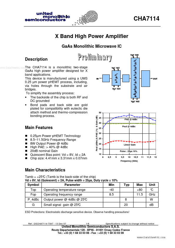
Pout (dBm) & PAE (%) & Gain (dB) CHA7114 is a monolithic two-stage GaAs high power amplifier designed for X band applications. This device is manufactured using a UMS 0.25 µm power pHEMT process, including, via holes through the substrate and air bridges. To simplify the assembly process: • The backside of the chip is both RF and DC grounded • Bond pads and back side are gold plated for compatibility with eutectic die attach method and thermo-compression bonding process. Vg1 Vd1 IN OUT Vg1 Vd1 Vg2 Vd2 50 45 40 35 30 25 20 15 Pulse : 25µs 10% 10 8 8,5 9 9,5 10 10,5 11 11,5 12 Frequency (GHz) Linear Gain Pout @ 4dBc PAE @ 4dBc Main Features 0.25µm Power pHEMT Technology 8.
Published: |