CHK8015-99F Description
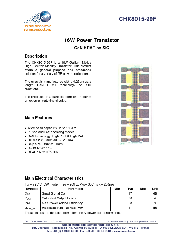
The CHK8015-99F is a 16W Gallium Nitride High Electron Mobility Transistor. This product offers a general purpose and broadband solution for a variety of RF power applications. The circuit is manufactured with a 0.25µm gate length GaN HEMT technology on SiC substrate.
CHK8015-99F Key Features
- Wide band capability up to 18GHz
- Pulsed and CW operating modes
- GaN technology: High Pout & High PAE
- DC bias: VD=30V @ID_Q=200mA
- Chip size 0.88x2x0.1mm
- RoHS N°2011/65
- REACh N°1907/2006
- 27 Oct 20
- Parc Mosaic
- 10, Avenue du Québec
CHK8015-99F Applications
- Wide band capability up to 18GHz