74HCT173 Overview
Key Specifications
Package: SOP
Pins: 16
Operating Voltage: 5 V
Max Voltage (typical range): 5.5 V
Description
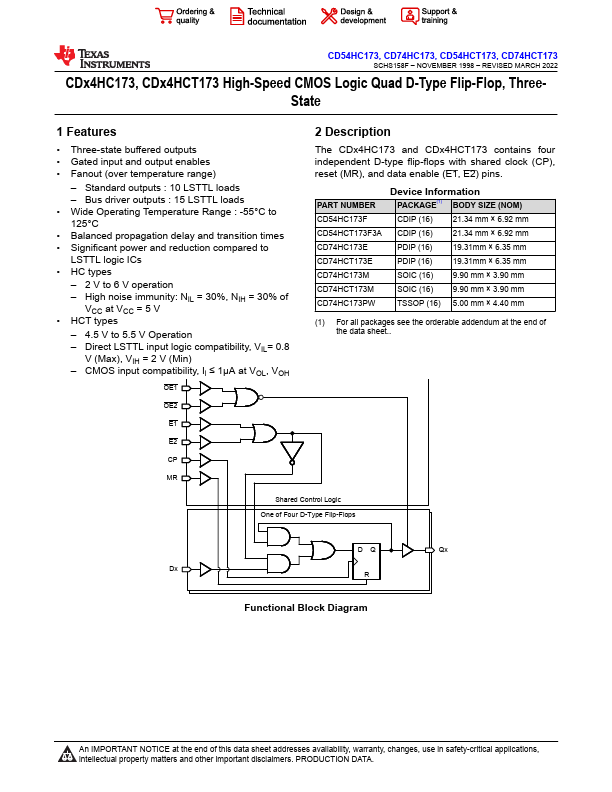
The CDx4HC173 and CDx4HCT173 contains four independent D-type flip-flops with shared clock (CP), reset (MR), and data enable (E1, E2) pins. PART NUMBER Device Information PACKAGE(1) BODY SIZE (NOM) CD54HC173F CDIP (16) 21.34 mm × 6.92 mm CD54HCT173F3A CDIP (16) 21.34 mm × 6.92 mm CD74HC173E PDIP (16) 19.31mm × 6.35 mm CD74HCT173E PDIP (16) 19.31mm × 6.35 mm CD74HC173M SOIC (16) 9.90 mm × 3.90 mm CD74HCT173M SOIC (16) 9.90 mm × 3.90 mm CD74HC173PW TSSOP (16) 5.00 mm × 4.40 mm (1) For all packages see the orderable addendum at the end of the data sheet.
Key Features
- Three-state buffered outputs
- Gated input and output enables
- Fanout (over temperature range) – Standard outputs : 10 LSTTL loads – Bus driver outputs : 15 LSTTL loads
- Wide Operating Temperature Range : -55°C to 125°C
- Balanced propagation delay and transition times