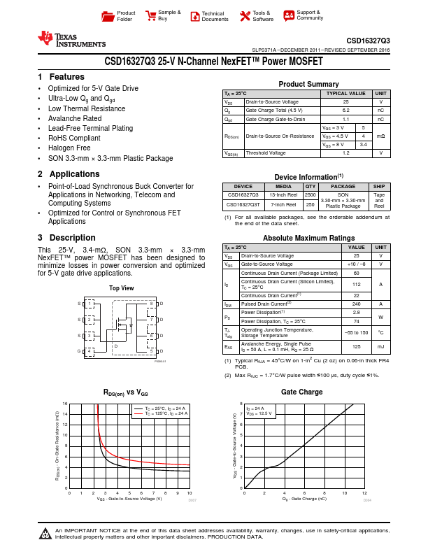
Datasheet4U Logo Datasheet4U.com

CSD16327Q3 - 25-V N-Channel Power MOSFET

General Description

This 25-V, 3.4-mΩ, SON 3.3-mm × 3.3-mm NexFET™ power MOSFET has been designed to minimize losses in power conversion and optimized for 5-V gate drive applications.

Key Features

  • 1 Optimized for 5-V Gate Drive.
  • Ultra-Low Qg and Qgd.
  • Low Thermal Resistance.
  • Avalanche Rated.
  • Lead-Free Terminal Plating.
  • RoHS Compliant.
  • Halogen Free.
  • SON 3.3-mm × 3.3-mm Plastic Package 2.

📥 Download Datasheet

Full PDF Text Transcription (Reference)

The following content is an automatically extracted verbatim text from the original manufacturer datasheet and is provided for reference purposes only.

View original datasheet text
Product Folder Sample & Buy Technical Documents Tools & Software Support & Community CSD16327Q3 SLPS371A – DECEMBER 2011 – REVISED SEPTEMBER 2016 CSD16327Q3 25-V N-Channel NexFET™ Power MOSFET 1 Features •1 Optimized for 5-V Gate Drive • Ultra-Low Qg and Qgd • Low Thermal Resistance • Avalanche Rated • Lead-Free Terminal Plating • RoHS Compliant • Halogen Free • SON 3.3-mm × 3.3-mm Plastic Package 2 Applications • Point-of-Load Synchronous Buck Converter for Applications in Networking, Telecom and Computing Systems • Optimized for Control or Synchronous FET Applications Product Summary TA = 25°C VDS Drain-to-Source Voltage Qg Gate Charge Total (4.5 V) Qgd Gate Charge Gate-to-Drain RDS(on) Drain-to-Source On-Resistance VGS(th) Threshold Voltage TYPICAL VALUE 25 6.2 1.