Datasheet Details
| Part number | AO3421E |
|---|---|
| Manufacturer | Alpha & Omega Semiconductors |
| File Size | 360.18 KB |
| Description | 30V P-Channel MOSFET |
| Datasheet |
 AO3421E Datasheet AO3421E Datasheet
|
|
|
| Part number | AO3421E |
|---|---|
| Manufacturer | Alpha & Omega Semiconductors |
| File Size | 360.18 KB |
| Description | 30V P-Channel MOSFET |
| Datasheet |
AO3421E Datasheet
|
|
|
|
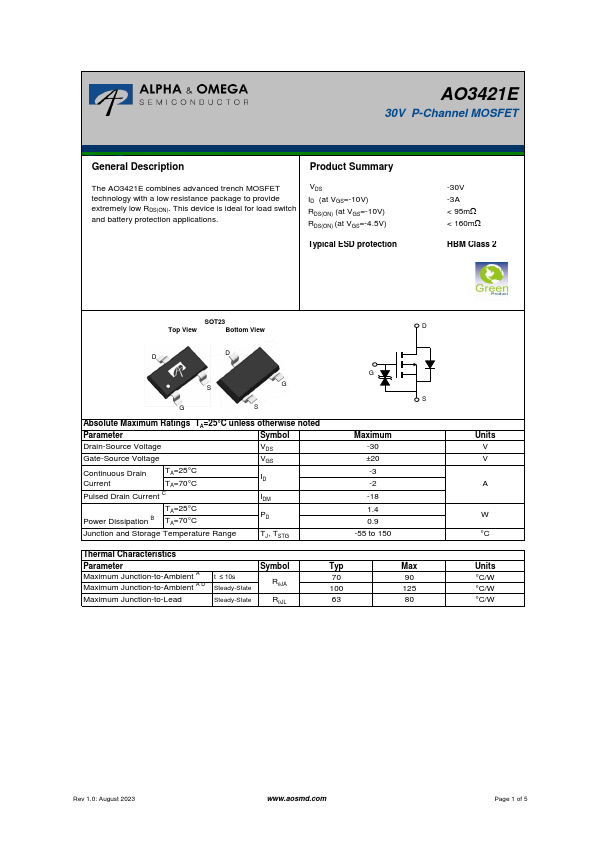
Product Summary The AO3421E combines advanced trench MOSFET technology with a low resistance package to provide extremely low RDS(ON).
This device is ideal for load switch and battery protection applications.
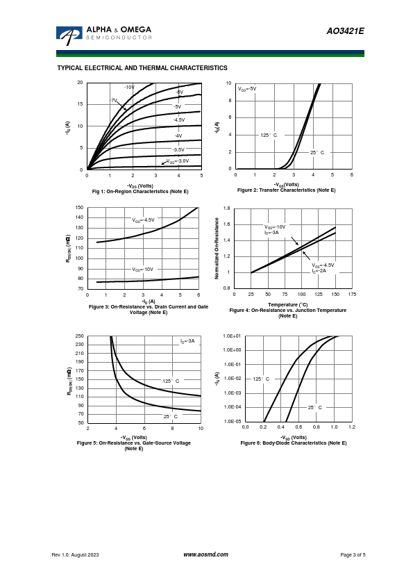
VDS ID (at VGS=-10V) RDS(ON) (at VGS=-10V) RDS(ON) (at VGS=-4.5V) Typical ESD protection -30V -3A < 95mW < 160mW HBM Class 2 SOT23 Top View Bottom View D D D S G G S Absolute Maximum Ratings TA=25°C unless otherwise noted Parameter Symbol Drain-Source Voltage VDS Gate-Source Voltage VGS Continuous Drain Current TA=25°C TA=70°C ID Pulsed Drain Current C IDM TA=25°C Power Dissipation B TA=70°C PD Junction and Storage Temperature Range TJ, TSTG G S Maximum -30 ±20 -3 -2 -18 1.4 0.9 -55 to 150 Thermal Characteristics Parameter Symbol Typ Maximum Junction-to-Ambient A t ≤ 10s Maximum Junction-to-Ambient A D Steady-State RqJA 70 100 Maximum Junction-to-Lead Steady-State RqJL 63 Max 90 125 80 Units V V A W °C Units °C/W °C/W °C/W Rev 1.0: August 2023 www.aosmd.com Page 1 of 5 AO3421E Electrical Characteristics (TJ=25°C unless otherwise noted) Symbol Parameter Conditions Min Typ Max Units STATIC PARAMETERS BVDSS Drain-Source Breakdown Voltage ID=-250mA, VGS=0V -30 V IDSS Zero Gate Voltage Drain Current VDS=-30V, VGS=0V TJ=55°C -1 mA -5 IGSS Gate-Body leakage current VDS=0V, VGS=±16V ±10 mA VGS(th) Gate Threshold Voltage VDS=VGS,ID=-250mA -1.4 -2 -2.5 V ID(ON) On state drain current VGS=-10V, VDS=-5V -18 A RDS(ON) Static Drain-Source On-Resistance VGS=-10V, ID=-3A TJ=125°C 78 95 mW 112 135 VGS=-4.5V, ID=-2A 120 160 mW gFS Forward Transconductance VDS=-5V, ID=-3A 6 S VSD Diode Forward Voltage IS=-1A,VGS=0V -0.8 -1 V IS Maximum Body-Diode Continuous Current -1.5 A DYNAMIC PARAMETERS Ciss Input Capacitance Coss Output Capacitance Crss Reverse Transfer Capacitance Rg Gate resistance VGS=0V, VDS=-15V, f=1MHz VGS=0V, VDS=0
AO3421E 30V P-Channel MOSFET General.
| Brand Logo | Part Number | Description | Manufacturer |
|---|---|---|---|
| AO3421E | P-Channel MOSFET | Kexin | |
| AO3421E-HF | P-Channel MOSFET | Kexin | |
| AO3421 | P-Channel MOSFET | Kexin |
| Part Number | Description |
|---|---|
| AO3421 | 30V P-Channel MOSFET |
| AO3420 | N-Channel MOSFET |
| AO3422 | N-Channel MOSFET |
| AO3423 | 20V P-Channel MOSFET |
| AO3424 | 30V N-Channel MOSFET |
| AO3400 | 30V N-Channel MOSFET |
| AO3400A | 30V N-Channel MOSFET |
| AO3401 | 30V P-Channel MOSFET |
| AO3401A | 30V P-Channel MOSFET |
| AO3401L | P-Channel MOSFET |