CY2305 Overview
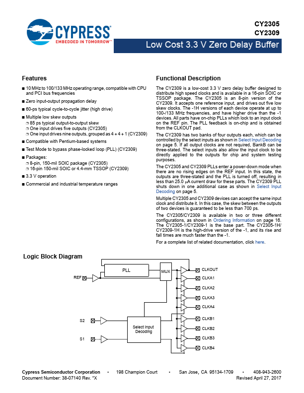
The CY2309 is a low-cost 3.3 V zero delay buffer designed to distribute high speed clocks and is available in a 16-pin SOIC or TSSOP package. The CY2305 is an 8-pin version of the CY2309. It accepts one reference input, and drives out five low skew clocks.
CY2305 Key Features
- 10 MHz to 100/133 MHz operating range, patible with CPU and PCI bus frequencies
- Zero input-output propagation delay
- 60-ps typical cycle-to-cycle jitter (high drive)
- Multiple low skew outputs
- 85 ps typical output-to-output skew
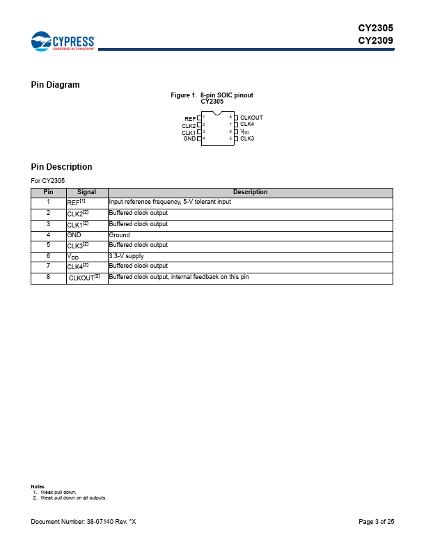
- One input drives five outputs (CY2305)
- One input drives nine outputs, grouped as 4 + 4 + 1 (CY2309)
- patible with Pentium-based systems
- Test Mode to bypass phase-locked loop (PLL) (CY2309)
- Packages