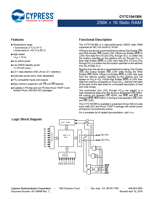
• Part: CY7C1041BN
  • Description: 256K x 16 Static RAM
  • Manufacturer: Cypress
  • Size: 442.50 KB
Download CY7C1041BN Datasheet PDF
CY7C1041BN page 2
Page 2
CY7C1041BN page 3
Page 3

CY7C1041BN Datasheet Text

CY7C1041BN 256K × 16 Static RAM 256K × 16 Static RAM Features - Temperature range: - mercial: 0 °C to 70 °C - Automotive-A: - 40 °C to 85 °C - High speed - tAA = 15 ns - Low active power - Low CMOS standby power - 2.75 mW (max.) - 2.0 V data retention (400 W at 2.0 V retention) - Automatic power-down when deselected - TTL-patible inputs and outputs - Easy memory expansion with CE and OE Features - Available in Pb-free and non Pb-free 44-pin TSOP II and molded 44-pin (400-Mil) SOJ packages Logic Block Diagram A0 A1 A2 AA34 A5 A6 AA78 Input Buffer 256K x 16 Array Column Decoder AAA19101 AA1123 A14 A15 A16 A17 Row Decoder Sense Amps Functional Description The CY7C1041BN is a high-performance CMOS static RAM organized as 262,144 words by 16 bits. Writing to the device is acplished by taking Chip Enable (CE) and Write Enable (WE) inputs LOW. If Byte Low Enable (BLE) is LOW, then data from I/O pins (I/O0 through I/O7), is written into the location specified on the address pins (A0 through A17). If Byte High Enable (BHE) is LOW, then data from I/O pins (I/O8 through I/O15) is written into the location specified on the address pins (A0 through A17). Reading from the device is acplished by taking Chip Enable (CE) and Output Enable (OE) LOW while forcing the Write Enable (WE) HIGH. If Byte Low Enable (BLE) is LOW, then data from the memory location specified by the address pins will appear on I/O0 to I/O7. If Byte High Enable (BHE) is LOW, then data from memory will appear on I/O8 to I/O15. See the truth table at the back of this data sheet for a plete description of read and write modes. The input/output pins (I/O0 through I/O15) are placed in a high-impedance state when the device is deselected (CE HIGH), the outputs are disabled (OE HIGH), the BHE and...