EDD2508AKTA-5-E
EDD2508AKTA-5-E is 256M bits DDR SDRAM (32M words x 8 bits DDR400) manufactured by Elpida Memory.
( Data Sheet : .. )
PRELIMINARY DATA SHEET
256M bits DDR SDRAM
EDD2508AKTA-5-E (32M words × 8 bits, DDR400)
Description
The EDD2508AKTA-5 is a 256M bits DDR SDRAM organized as 8,388,608 words × 8 bits × 4 banks. Read and write operations are performed at the cross points of the CK and the /CK. This high-speed data transfer is realized by the 2 bits prefetch-pipelined architecture. Data strobe (DQS) both for read and write are available for high speed and reliable data bus design. By setting extended mode register, the on-chip Delay Locked Loop (DLL) can be set enable or disable. It is packaged in 66-pin plastic TSOP (II).
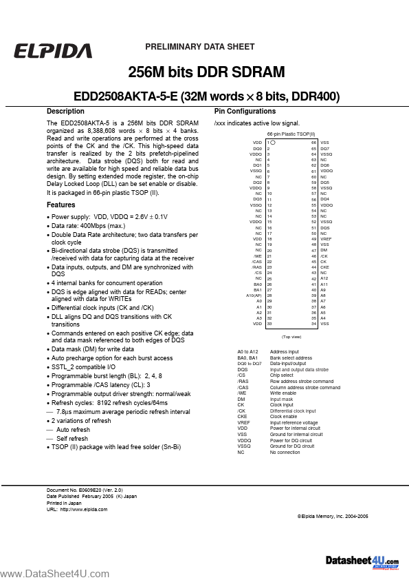
Pin Configurations
/xxx indicates active low signal.
66-pin Plastic TSOP(II)
VDD DQ0 VDDQ NC DQ1 VSSQ NC DQ2 VDDQ NC DQ3 VSSQ NC NC VDDQ NC NC VDD NC NC /WE /CAS /RAS /CS NC BA0 BA1 A10(AP) A0 A1 A2 A3 VDD
Features
- Power supply: VDD, VDDQ = 2.6V ± 0.1V
- Data rate: 400Mbps (max.)
- Double Data Rate architecture; two data transfers per clock cycle
- Bi-directional data strobe (DQS) is transmitted /received with data for capturing data at the receiver
- Data inputs, outputs, and DM are synchronized with DQS
- 4 internal banks for concurrent operation
- DQS is edge aligned with data for READs; center aligned with data for WRITEs
- Differential clock inputs (CK and /CK)
- DLL aligns DQ and DQS transitions with CK transitions
- mands entered on each positive CK edge; data and data mask referenced to both edges of DQS
- Data mask (DM) for write data
- Auto precharge option for each burst access
- SSTL_2 patible I/O
- Programmable burst length (BL): 2, 4, 8
- Programmable /CAS latency (CL): 3
- Programmable output driver strength: normal/weak
- Refresh cycles: 8192 refresh cycles/64ms 7.8µs maximum average periodic refresh interval
- 2 variations of refresh Auto refresh Self refresh
- TSOP (II) package with lead free solder...