EMP38K03HPC
EMP38K03HPC is Dual N-Channel Logic Level Enhancement Mode Field Effect Transistor manufactured by Excelliance MOS.
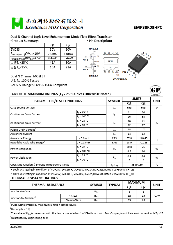
Dual N-Channel Logic Level Enhancement Mode Field Effect Transistor
- Product Summary:
- Pin Description:
Q1
Q2
BVDSS
30V
30V
RDSON (MAX.)@VGS=10V RDSON (MAX.)@VGS=4.5V ID @TC=25℃
7.0mΩ 9.4mΩ
41A
4.0mΩ 5.4mΩ
60A
ID @TA=25℃
16A
21A
Dual N Channel MOSFET UIS, Rg 100% Tested RoHS & Halogen Free & TSCA pliant
-...