MD7IC21100NR1
Key Features
- 100% PAR Tested for Guaranteed Output Power Capability
- On - Chip Matching (50 Ohm Input, on a per side basis, DC Blocked)
- Internally Matched for Ease of Use
- Integrated Quiescent Current Temperature pensation with Enable/ Disable Function (1)
- Integrated ESD Protection
- 225°C Capable Plastic Package
- In Tape and Reel. R1 Suffix = 500 Units per 44 mm, 13 inch Reel
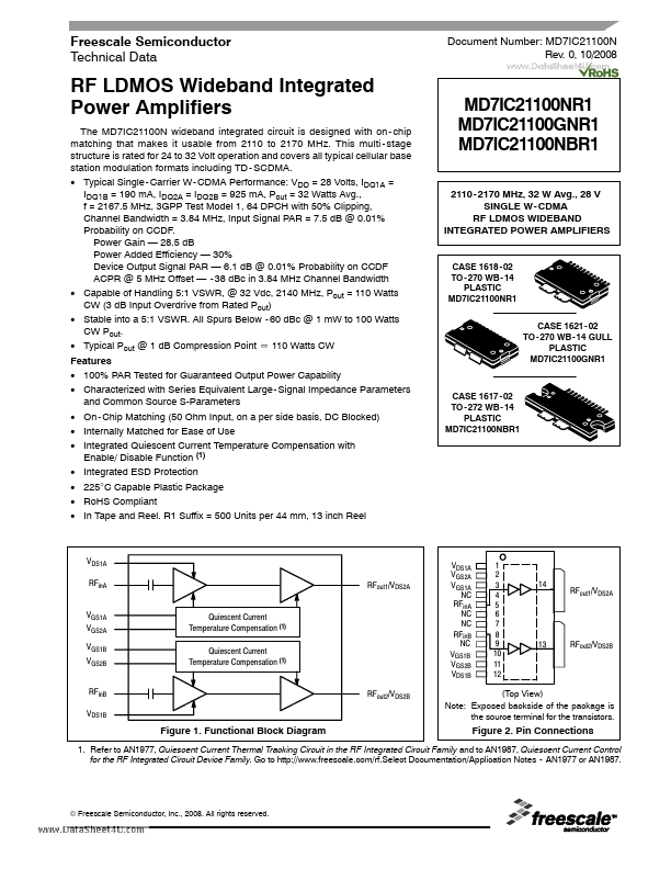
- Functional Figure
- All rights reserved
- Characteristic Table