Part number:
HD74CDCF2510B
Manufacturer:
Hitachi Semiconductor
File Size:
43.42 KB
Description:
140 mhz/ 0 to 85c operation 3.3-v phase-lock loop clock driver.
HD74CDCF2510B Features
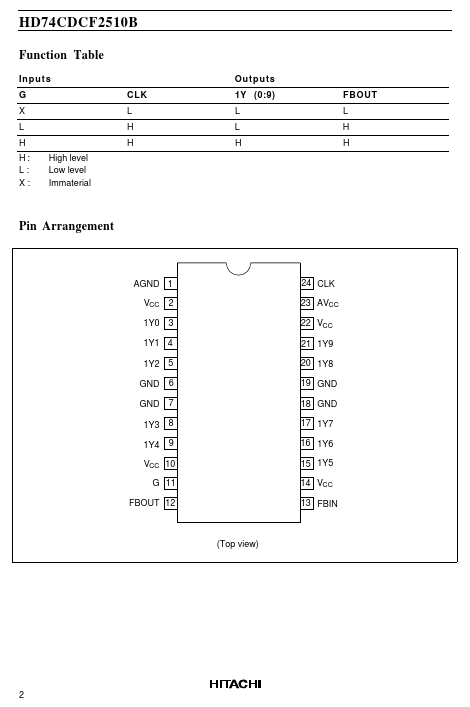
* Supports PC133 and meets “PC SDRAM registered DIMM specification, Rev. 1.1” Phase-lock loop clock distribution for synchronous DRAM applications External feedback (FBIN) pin is used to synchronize the outputs to the clock input No
HD74CDCF2510B Datasheet (43.42 KB)
Datasheet Details
HD74CDCF2510B
Hitachi Semiconductor
43.42 KB
140 mhz/ 0 to 85c operation 3.3-v phase-lock loop clock driver.
📁 Related Datasheet
HD74CDCF2510B 3.3-V Phase-lock Loop Clock Driver (Renesas)
HD74CDCF2509B 140 MHz/ 0 to 85C Operation 3.3-V Phase-lock Loop Clock Driver (Hitachi Semiconductor)
HD74CDCF2509B 3.3-V Phase-lock Loop Clock Driver (Renesas)
HD74CDC2509B 3.3-V Phase-lock Loop Clock Driver (Hitachi Semiconductor)
HD74CDC2509B 3.3-V Phase-lock Loop Clock Driver (Renesas)
HD74CDC2510B 3.3-V Phase-lock Loop Clock Driver (Hitachi Semiconductor)
HD74CDC2510B 3.3-V Phase-lock Loop Clock Driver (Renesas)
HD74CDC857 3.3/2.5-V Phase-lock Loop Clock Driver (Hitachi Semiconductor)
HD74CDCF2510B Distributor