HY5DU281622 Overview
Description
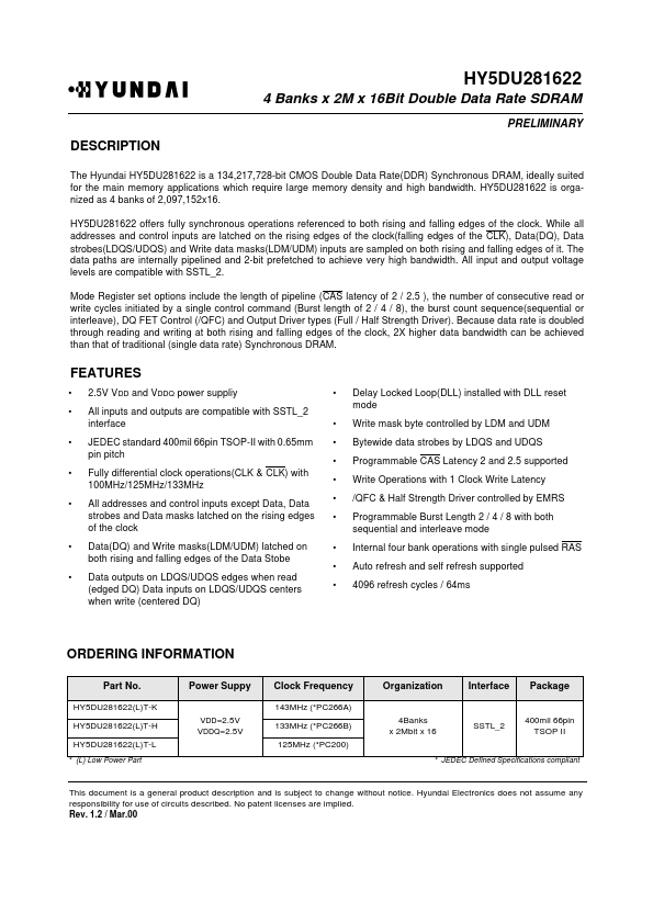
The Hyundai HY5DU281622 is a 134,217,728-bit CMOS Double Data Rate(DDR) Synchronous DRAM, ideally suited for the main memory applications which require large memory density and high bandwidth. HY5DU281622 is organized as 4 banks of 2,097,152x16.
Key Features
- Delay Locked Loop(DLL) instal