SY89873L
SY89873L is IN-TO-LVDS PROGRAMMABLE CLOCK DIVIDER FANOUT BUFFER W/ INTERNAL TERMINATION manufactured by Micrel Semiconductor.
Micrel, Inc.
3.3V, 2.0GHz ANY DIFF. IN-TO-LVDS SY89873L ® Precision Edge PROGRAMMABLE CLOCK DIVIDER SY89873L FANOUT BUFFER W/ INTERNAL TERMINATION
Precision Edge®
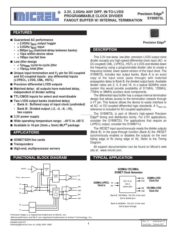
Features
- Guaranteed AC performance Precision Edge®
- > 2.0GHz fMAX output toggle
- > 3.0GHz fMAX input DESCRIPTION
- < 800ps tPD (matched-delay between banks)
- < 15ps within-device skew This 3.3V low-skew, low-jitter, precision LVDS output clock
- < 190ps rise/fall time divider accepts any high-speed differential clock input (AC- or
- Low jitter design DC-coupled) CML, LVPECL, HSTL or LVDS and divides down
- < 1psRMS cycle-to-cycle jitter the frequency using a programmable divider ratio to create a
- < 10psPP total jitter...