Datasheet Summary
MOTOROLA
SEMICONDUCTOR TECHNICAL DATA
Order this document by MMFT108T1/D
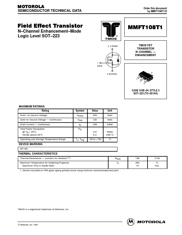
Field Effect Transistor
N- Channel Enhancement- Mode Logic Level SOT- 223
®
2, 4 DRAIN
TMOS FET TRANSISTOR N- CHANNEL
- ENHANCEMENT
1 GATE 3 SOURCE
1 2 3 4
CASE 318E- 04, STYLE 3 SOT- 223 (TO- 261AA)
MAXIMUM RATINGS
Rating Drain
- to- Source Voltage Gate- to- Source Voltage
- Continuous Drain Current
- Continuous Total Power Dissipation @ TA = 25°C Derate above 25°C Operating and Storage Temperature Range Symbol VDSS VGS ID PD 0.8 6.4 TJ, Tstg
- 65 to +150 Watts mW/°C °C Value 200 ±20 250 Unit Volts Volts mAdc
DEVICE MARKING
MT108
THERMAL CHARACTERISTICS
Thermal Resistance
- Junction- to- Ambient (1) Maximum...