Datasheet4U Logo Datasheet4U.com

FDG6301N - Dual N-Channel Digital FET

Datasheet Summary

Description

These dual N

transistors are produced using onsemi’s proprietary, high cell density, DMOS technology.

state resistance.

Features

  • 25 V, 0.22 A Continuous, 0.65 A Peak  RDS(ON) = 4 W @ VGS = 4.5 V  RDS(ON) = 5 W @ VGS = 2.7 V.
  • Very Low Level Gate Drive Requirements Allowing Direct Operation in 3 V Circuits (VGS(th) < 1.5 V).
  • Gate.
  • Source Zener for ESD Ruggedness (>6 kV Human Body Model).
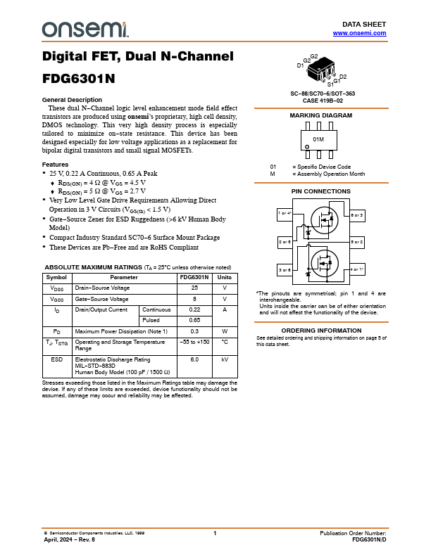
  • Compact Industry Standard SC70.
  • 6 Surface Mount Package.
  • These Devices are Pb.
  • Free and are RoHS Compliant.

📥 Download Datasheet

Datasheet preview – FDG6301N

Datasheet Details

Part number FDG6301N
Manufacturer ON Semiconductor
File Size 233.56 KB
Description Dual N-Channel Digital FET
Datasheet download datasheet FDG6301N Datasheet
Additional preview pages of the FDG6301N datasheet.
Other Datasheets by ON Semiconductor

Full PDF Text Transcription

Click to expand full text
Digital FET, Dual N-Channel FDG6301N General Description These dual N−Channel logic level enhancement mode field effect transistors are produced using onsemi’s proprietary, high cell density, DMOS technology. This very high density process is especially tailored to minimize on−state resistance. This device has been designed especially for low voltage applications as a replacement for bipolar digital transistors and small signal MOSFETs. Features  25 V, 0.22 A Continuous, 0.65 A Peak  RDS(ON) = 4 W @ VGS = 4.5 V  RDS(ON) = 5 W @ VGS = 2.7 V  Very Low Level Gate Drive Requirements Allowing Direct Operation in 3 V Circuits (VGS(th) < 1.
Published: |