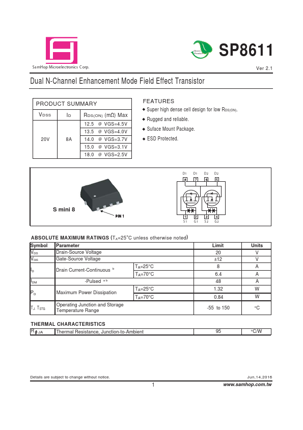
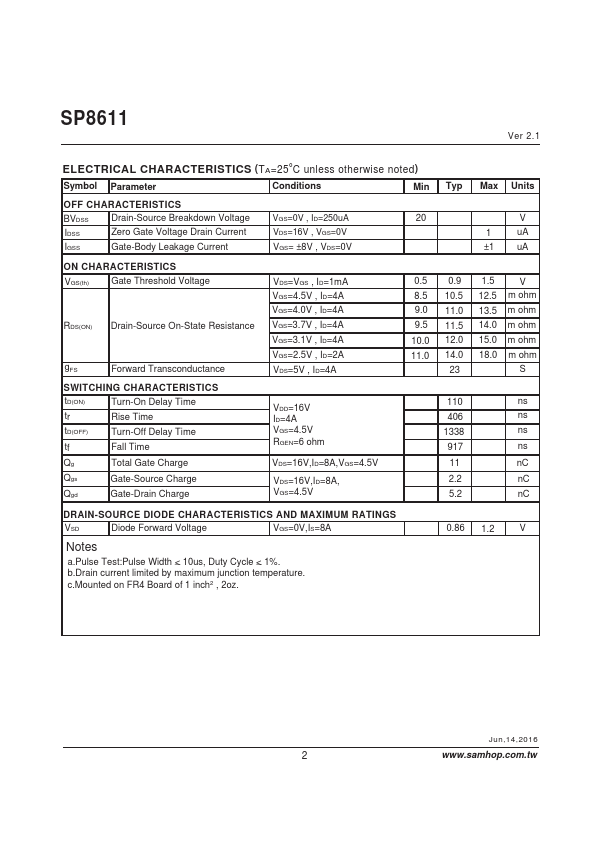
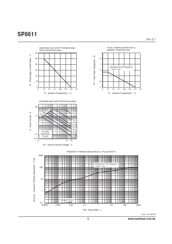
SP8611 Overview
Green Product Sa mHop Microelectronics C orp.
SP8611 datasheet by SamHop Microelectronics.
| Part number | SP8611 |
|---|---|
| Datasheet | SP8611-SamHopMicroelectronics.pdf |
| File Size | 73.50 KB |
| Manufacturer | SamHop Microelectronics |
| Description | Dual N-Channel Enhancement Mode Field Effect Transistor |
|
|
Green Product Sa mHop Microelectronics C orp.
| Brand Logo | Part Number | Description | Other Manufacturers |
|---|---|---|---|
| SP8611 | asynchronous ECL divide | Zarlink Semiconductor |
View all SamHop Microelectronics datasheets
| Part Number | Description |
|---|---|
| SP8610 | Dual N-Channel Enhancement Mode Field Effect Transistor |
| SP8601 | Dual N-Channel Enhancement Mode Field Effect Transistor |
| SP8608 | Dual N-Channel Enhancement Mode Field Effect Transistor |
| SP8651 | Dual N-Channel Enhancement Mode Field Effect Transistor |
| SP8005 | N-Channel Enhancement Mode Field Effect Transistor |
| SP8006 | N-Channel Enhancement Mode Field Effect Transistor |
| SP8007 | N-Channel Enhancement Mode Field Effect Transistor |
| SP8008 | N-Channel Enhancement Mode Field Effect Transistor |
| SP8009 | N-Channel Enhancement Mode Field Effect Transistor |
| SP8009E | N-Channel Enhancement Mode Field Effect Transistor |