30J301 Description
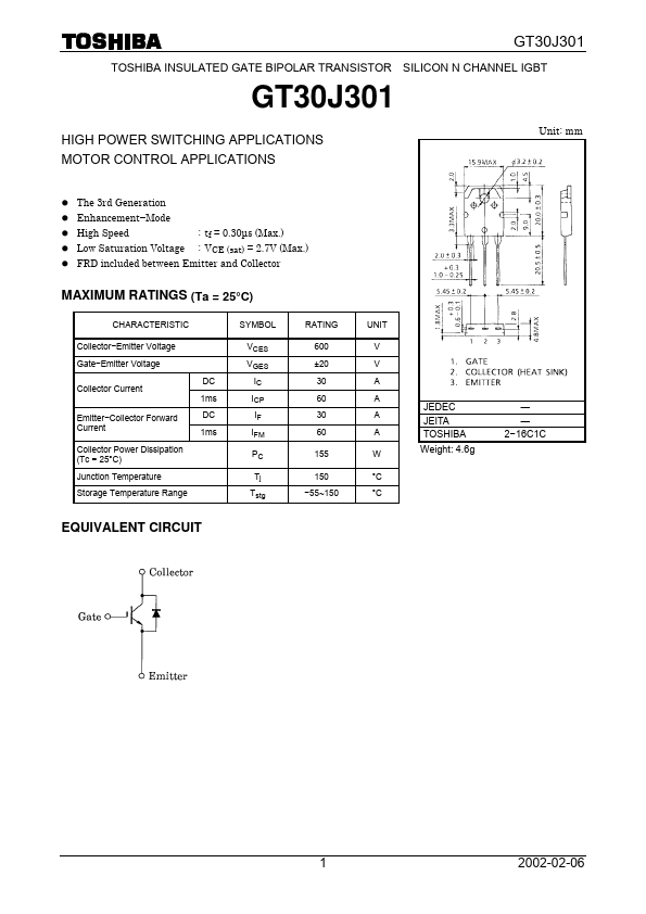
GT30J301 TOSHIBA INSULATED GATE BIPOLAR TRANSISTOR SILICON N CHANNEL IGBT GT30J301 HIGH POWER SWITCHING APPLICATIONS MOTOR CONTROL APPLICATIONS Unit: mm l The 3rd Generation l Enhancement−Mode l High Speed : tf = 0.30µs (Max.) l Low Saturation Voltage.
30J301 Key Features
- The 3rd Generation
- Enhancement−Mode
- High Speed : tf = 0.30µs (Max.)
- Low Saturation Voltage : VCE (sat) = 2.7V (Max.)
- FRD included between Emitter and Collector MAXIMUM RATINGS (Ta = 25°C) CHARACTERISTIC Collector−Emitter Vol