Datasheet4U Logo Datasheet4U.com

WED2ZLRSP01S - Dual Array Synchronous Pipeline Burst NBL SRAM

Description

The WED2ZLRSP01S, Dual Independent Array, NBLSSRAM device employs high-speed, Low-Power CMOS silicon and is fabricated using an advanced CMOS process.

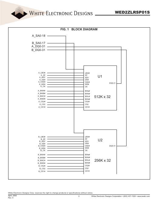
WEDC’s 24Mb, Sync Burst SRAM MCP integrates two totally independent arrays, the first organized as a 512K x 32, and the second a 256K x 32.

Features

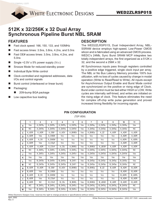
  • Fast clock speed: 166, 150, 133, and 100MHz Fast access times: 3.5ns, 3.8ns, 4.2ns, and 5.0ns Fast OE# access times: 3.5ns, 3.8ns, 4.2ns, and 5.0ns Single +2.5V ± 5% power supply (VCC) Snooze Mode for reduced-standby power Individual Byte Write control Clock-controlled and registered addresses, data I/Os and control signals Burst control (interleaved or linear burst) Packaging: 209-bump BGA package Low capacitive bus loading WED2ZLRSP01S.

📥 Download Datasheet

Datasheet Details

Part number WED2ZLRSP01S
Manufacturer White Electronic
File Size 376.33 KB
Description Dual Array Synchronous Pipeline Burst NBL SRAM
Datasheet download datasheet WED2ZLRSP01S Datasheet

Full PDF Text Transcription

Click to expand full text
www.DataSheet4U.com White Electronic Designs 512K x 32/256K x 32 Dual Array Synchronous Pipeline Burst NBL SRAM FEATURES Fast clock speed: 166, 150, 133, and 100MHz Fast access times: 3.5ns, 3.8ns, 4.2ns, and 5.0ns Fast OE# access times: 3.5ns, 3.8ns, 4.2ns, and 5.0ns Single +2.5V ± 5% power supply (VCC) Snooze Mode for reduced-standby power Individual Byte Write control Clock-controlled and registered addresses, data I/Os and control signals Burst control (interleaved or linear burst) Packaging: 209-bump BGA package Low capacitive bus loading WED2ZLRSP01S DESCRIPTION The WED2ZLRSP01S, Dual Independent Array, NBLSSRAM device employs high-speed, Low-Power CMOS silicon and is fabricated using an advanced CMOS process.
Published: |