Datasheet Details
| Part number | AO3410 |
|---|---|
| Manufacturer | Alpha & Omega Semiconductors |
| File Size | 162.19 KB |
| Description | N-Channel MOSFET |
| Datasheet |
 AO3410 Datasheet AO3410 Datasheet
|
|
|
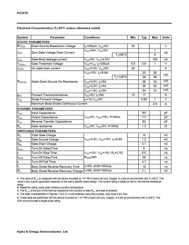
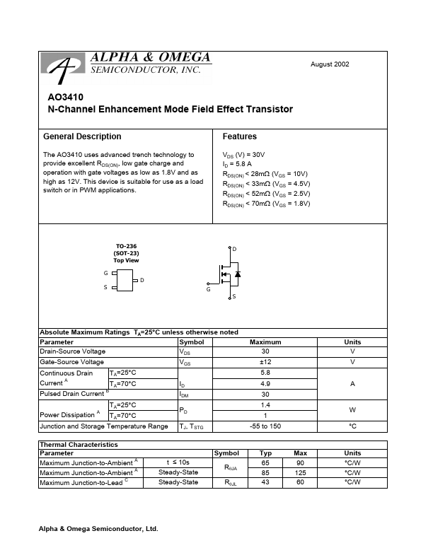
The AO3410 uses advanced trench technology to provide excellent RDS(ON), low gate charge and operation with gate voltages as low as 1.8V and as high as 12V.
This device is suitable for use as a load switch or in PWM applications.
| Part number | AO3410 |
|---|---|
| Manufacturer | Alpha & Omega Semiconductors |
| File Size | 162.19 KB |
| Description | N-Channel MOSFET |
| Datasheet |
AO3410 Datasheet
|
|
|
|