Datasheet Details
| Part number | AO3413 |
|---|---|
| Manufacturer | Alpha & Omega Semiconductors |
| File Size | 247.86 KB |
| Description | 20V P-Channel MOSFET |
| Datasheet |
 AO3413 Datasheet AO3413 Datasheet
|
|
|
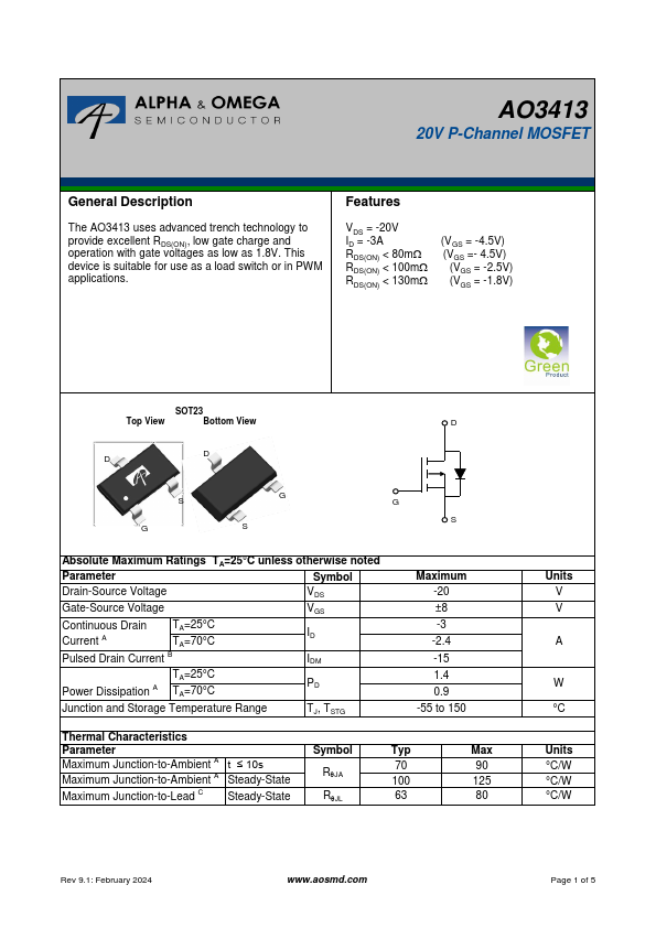
The AO3413 uses advanced trench technology to provide excellent RDS(ON), low gate charge and operation with gate voltages as low as 1.8V.
This device is suitable for use as a load switch or in PWM applications.
| Part number | AO3413 |
|---|---|
| Manufacturer | Alpha & Omega Semiconductors |
| File Size | 247.86 KB |
| Description | 20V P-Channel MOSFET |
| Datasheet |
AO3413 Datasheet
|
|
|
|