Low on-resistance R DS =1.26 Ω typ. (V GS = 10 V , ID = 150 mA) R DS = 2.8 Ω typ. (VGS = 4 V , ID = 50 mA).
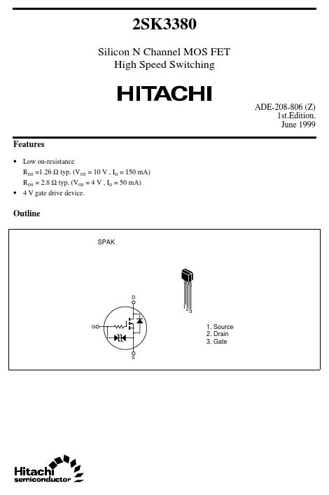
4 V gate drive device. Outline
SPAK
D
12 3
G
1. Source 2. Drain 3. Gate
S
2SK3380
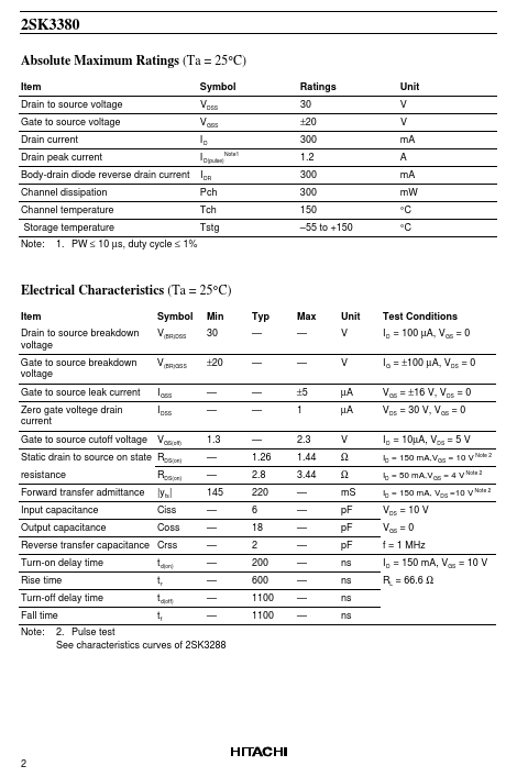
Absolute Maximum Ratings (Ta = 25°C)
Item Drain to source voltage Gate to source voltage Drain current Drain peak current Body-drain diode reverse drain current Channel dissipation Channel temperature Storage temperature Note: 1. PW ≤ 10 µs, duty cycle ≤ 1% Symbol VDSS VGSS ID I D(pul.
 2SK3380_HitachiSemiconductor.pdf