Datasheet Details
| Part number | HD74ALVCH16831 |
|---|---|
| Manufacturer | Hitachi Semiconductor |
| File Size | 60.23 KB |
| Description | 1-to 4 Address Register / Driver with 3-state Outputs |
| Datasheet |
 HD74ALVCH16831 Datasheet HD74ALVCH16831 Datasheet
|
|
|
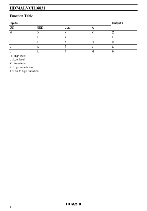
This 1-bit to 4-bit address register / driver is designed for 2.3 V to 3.6 V VCC operation.
The device is ideal for use in applications in which a single address bus is driving four separate memory locations.
| Part number | HD74ALVCH16831 |
|---|---|
| Manufacturer | Hitachi Semiconductor |
| File Size | 60.23 KB |
| Description | 1-to 4 Address Register / Driver with 3-state Outputs |
| Datasheet |
HD74ALVCH16831 Datasheet
|
|
|
|