Datasheet4U Logo Datasheet4U.com

H55S2562JFR-75M, H55S2562JFR-60M Datasheet - Hynix Semiconductor

H55S2562JFR-75M - 256MBit MOBILE SDR SDRAM based on 4M x 4Bank x16 I/O

and is subject to change without notice.

Hynix does not assume any responsibility for use of circuits described.

No patent licenses are implied.

Rev 1.1 / July.

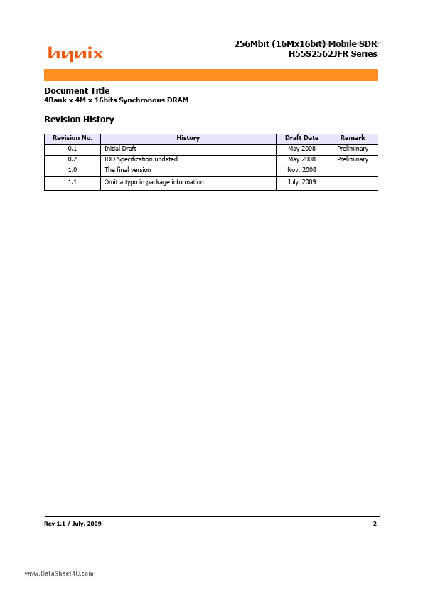
2009 1 11 www.DataSheet4U.com 256Mbit (16Mx16bit) Mobile SDR H55S2562JFR Series Document Title 4Bank x 4M x 16bits Synchronous DRAM Revi

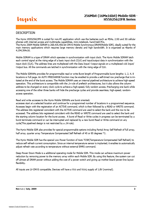
H55S2562JFR-75M Features

* Standard SDRAM Protocol Clock Synchronization Operation - All the commands registered on positive edge of basic input clock (CLK) MULTIBANK OPERATION - Internal 4bank operation - During burst Read or Write operation, burst Read or Write for a different bank is performed. - During b

H55S2562JFR-60M_HynixSemiconductor.pdf

This datasheet PDF includes multiple part numbers: H55S2562JFR-75M, H55S2562JFR-60M. Please refer to the document for exact specifications by model.
H55S2562JFR-75M Datasheet Preview Page 2 H55S2562JFR-75M Datasheet Preview Page 3

Datasheet Details

Part number:

H55S2562JFR-75M, H55S2562JFR-60M

Manufacturer:

Hynix Semiconductor

File Size:

751.58 KB

Description:

256mbit mobile sdr sdram based on 4m x 4bank x16 i/o.

Note:

This datasheet PDF includes multiple part numbers: H55S2562JFR-75M, H55S2562JFR-60M.
Please refer to the document for exact specifications by model.

📁 Related Datasheet

📌 All Tags