Datasheet Details
- Part number
- IDTCSP2510C
- Manufacturer
- Integrated Device
- File Size
- 63.40 KB
- Datasheet
- IDTCSP2510C_IntegratedDeviceTechnology.pdf
- Description
- 3.3V PHASE-LOCK LOOP CLOCK DRIVER ZERO DELAY BUFFER
IDTCSP2510C Description
IDTCSP2510C 3.3V PHASE-LOCK LOOP CLOCK DRIVER 0ºC TO 85ºC TEMPERATURE RANGE 3.3V PHASE-LOCK LOOP CLOCK DRIVER ZERO DELAY BUFFER .
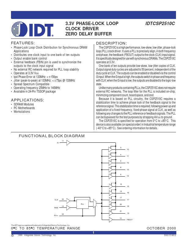
FUNCTIONAL BLOCK DIAGRAM
11 G 3 Y0 4 Y1 5 Y2 8 Y3 9 Y4
15 Y5 16 Y6 17 CLK 24 PLL 13 FBIN 21 AV DD 23 12 FBOUT Y9 20 Y8 Y7
ºC TEMPERATURE RANGE 0º.
IDTCSP2510C Applications
* Distributes one clock input to one bank of ten outputs
* Output enable bank control
* External feedback (FBIN) pin is used to synchronize the outputs to the clock input signal
* No external RC network required for PLL loop stability
* Operates at 3.3V VDD
📁 Related Datasheet
📌 All Tags
IDTCSP2510C Stock/Price