Datasheet Details
- Part number
- M28F010
- Manufacturer
- Intel Corporation
- File Size
- 317.31 KB
- Datasheet
- M28F010_IntelCorporation.pdf
- Description
- 1024K (128K x 8) CMOS FLASH MEMORY
M28F010 Description
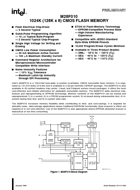
M28F010 1024K (128K x 8) CMOS FLASH MEMORY Y Y Y Y Y Flash Electrical Chip-Erase 5 Second Typical Quick-Pulse Programming Algorithm 10 ms Typical.
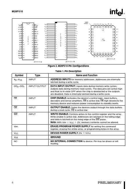
Symbol A0.
A16 DQ0.
DQ7 Type INPUT INPUT OUTPUT Name and Function ADDRESS INPUTS for memory addresses Addresses are internally latched.
M28F010 Features
* g 10% VCC Tolerance Maximum Latch-Up Immunity through EPI Processing
Y
Y
Y Y
ETOX-III Flash-Memory Technology EPROM-Compatible Process Base High-Volume Manufacturing Experience Compatible with JEDEC-Standard Byte-Wide EPROM Pinouts 10 000 Program Erase Cycles Minimum Available in Three Product G
M28F010 Applications
* where traditional EEPROM functionality (byte erasure) is either not required or is not cost-effective Use of the M28F010 is also appropriate where EPROM ultraviolet erasure is impractical or too time consuming
271111
* 1
Figure 1 M28F010 Block Diagram
January 1996
Order Number 271111-005
📁 Related Datasheet
📌 All Tags